- 您現(xiàn)在的位置:買(mǎi)賣(mài)IC網(wǎng) > PDF目錄4460 > A42MX09-TQG176A (Microsemi SoC)IC FPGA MX SGL CHIP 14K 176-TQFP PDF資料下載
參數(shù)資料
| 型號(hào): | A42MX09-TQG176A |
| 廠商: | Microsemi SoC |
| 文件頁(yè)數(shù): | 96/142頁(yè) |
| 文件大?。?/td> | 0K |
| 描述: | IC FPGA MX SGL CHIP 14K 176-TQFP |
| 標(biāo)準(zhǔn)包裝: | 40 |
| 系列: | MX |
| 輸入/輸出數(shù): | 104 |
| 門(mén)數(shù): | 14000 |
| 電源電壓: | 3 V ~ 3.6 V,4.5 V ~ 5.5 V |
| 安裝類(lèi)型: | 表面貼裝 |
| 工作溫度: | -40°C ~ 125°C |
| 封裝/外殼: | 176-LQFP |
| 供應(yīng)商設(shè)備封裝: | 176-TQFP(24x24) |
第1頁(yè)第2頁(yè)第3頁(yè)第4頁(yè)第5頁(yè)第6頁(yè)第7頁(yè)第8頁(yè)第9頁(yè)第10頁(yè)第11頁(yè)第12頁(yè)第13頁(yè)第14頁(yè)第15頁(yè)第16頁(yè)第17頁(yè)第18頁(yè)第19頁(yè)第20頁(yè)第21頁(yè)第22頁(yè)第23頁(yè)第24頁(yè)第25頁(yè)第26頁(yè)第27頁(yè)第28頁(yè)第29頁(yè)第30頁(yè)第31頁(yè)第32頁(yè)第33頁(yè)第34頁(yè)第35頁(yè)第36頁(yè)第37頁(yè)第38頁(yè)第39頁(yè)第40頁(yè)第41頁(yè)第42頁(yè)第43頁(yè)第44頁(yè)第45頁(yè)第46頁(yè)第47頁(yè)第48頁(yè)第49頁(yè)第50頁(yè)第51頁(yè)第52頁(yè)第53頁(yè)第54頁(yè)第55頁(yè)第56頁(yè)第57頁(yè)第58頁(yè)第59頁(yè)第60頁(yè)第61頁(yè)第62頁(yè)第63頁(yè)第64頁(yè)第65頁(yè)第66頁(yè)第67頁(yè)第68頁(yè)第69頁(yè)第70頁(yè)第71頁(yè)第72頁(yè)第73頁(yè)第74頁(yè)第75頁(yè)第76頁(yè)第77頁(yè)第78頁(yè)第79頁(yè)第80頁(yè)第81頁(yè)第82頁(yè)第83頁(yè)第84頁(yè)第85頁(yè)第86頁(yè)第87頁(yè)第88頁(yè)第89頁(yè)第90頁(yè)第91頁(yè)第92頁(yè)第93頁(yè)第94頁(yè)第95頁(yè)當(dāng)前第96頁(yè)第97頁(yè)第98頁(yè)第99頁(yè)第100頁(yè)第101頁(yè)第102頁(yè)第103頁(yè)第104頁(yè)第105頁(yè)第106頁(yè)第107頁(yè)第108頁(yè)第109頁(yè)第110頁(yè)第111頁(yè)第112頁(yè)第113頁(yè)第114頁(yè)第115頁(yè)第116頁(yè)第117頁(yè)第118頁(yè)第119頁(yè)第120頁(yè)第121頁(yè)第122頁(yè)第123頁(yè)第124頁(yè)第125頁(yè)第126頁(yè)第127頁(yè)第128頁(yè)第129頁(yè)第130頁(yè)第131頁(yè)第132頁(yè)第133頁(yè)第134頁(yè)第135頁(yè)第136頁(yè)第137頁(yè)第138頁(yè)第139頁(yè)第140頁(yè)第141頁(yè)第142頁(yè)
40MX and 42MX FPGA Families
Re vi s i on 11
1 - 53
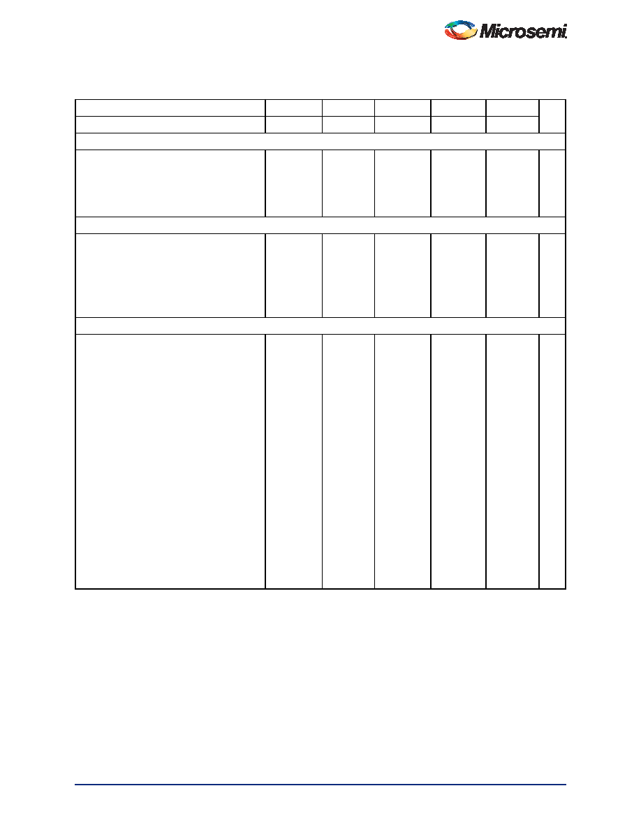
Input Module Propagation Delays
tINYH
Pad-to-Y HIGH
1.0
1.2
1.3
1.6
2.2
ns
tINYL
Pad-to-Y LOW
0.8
0.9
1.0
1.2
1.7
ns
tINGH
G to Y HIGH
1.3
1.4
1.6
1.9
2.7
ns
tINGL
G to Y LOW
1.3
1.4
1.6
1.9
2.7
ns
Input Module Predicted Routing Delays2
tIRD1
FO = 1 Routing Delay
2.0
2.2
2.5
3.0
4.2
ns
tIRD2
FO = 2 Routing Delay
2.3
2.5
2.9
3.4
4.7
ns
tIRD3
FO = 3 Routing Delay
2.5
2.8
3.2
3.7
5.2
ns
tIRD4
FO = 4 Routing Delay
2.8
3.1
3.5
4.1
5.7
ns
tIRD8
FO = 8 Routing Delay
3.7
4.1
4.7
5.5
7.7
ns
Global Clock Network
tCKH
Input LOW to HIGH
FO = 32
FO = 256
2.4
2.7
3.0
3.4
3.6
4.0
5.0
5.5
ns
tCKL
Input HIGH to LOW
FO = 32
FO = 256
3.5
3.9
4.3
4.4
4.9
5.2
5.7
7.3
8.0
ns
tPWH
Minimum Pulse
Width HIGH
FO = 32
FO = 256
1.2
1.3
1.4
1.5
1.7
1.8
2.0
2.5
2.7
ns
tPWL
Minimum Pulse
Width LOW
FO = 32
FO = 256
1.2
1.3
1.4
1.5
1.7
1.8
2.0
2.5
2.7
ns
tCKSW
Maximum Skew
FO = 32
FO = 256
0.3
0.4
0.5
0.6
ns
tSUEXT
Input Latch
External Set-Up
FO = 32
FO = 256
0.0
ns
tHEXT
Input Latch
External Hold
FO = 32
FO = 256
2.3
2.2
2.6
2.4
3.0
3.3
3.5
3.9
4.9
5.5
ns
tP
Minimum Period
FO = 32
FO = 256
3.4
3.7
4.1
4.0
4.5
4.7
5.2
7.8
8.6
ns
fMAX
Maximum Frequency FO = 32
FO = 256
296
268
269
244
247
224
215
195
129
117
MHz
Table 1-32 A42MX09 Timing Characteristics (Nominal 5.0 V Operation) (continued)
(Worst-Case Commercial Conditions, VCCA = 4.75 V, TJ = 70°C)
–3 Speed
–2 Speed
–1 Speed
Std Speed
–F Speed
Units
Parameter / Description
Min. Max. Min. Max. Min. Max. Min. Max. Min. Max.
Notes:
1. For dual-module macros, use tPD1 + tRD1 + tPDn, tCO + tRD1 + tPDn, or tPD1 + tRD1 + tSUD, whichever is appropriate.
2. Routing delays are for typical designs across worst-case operating conditions. These parameters should be used for
estimating device performance. Post-route timing analysis or simulation is required to determine actual performance.
3. Data applies to macros based on the S-module. Timing parameters for sequential macros constructed from C-modules
can be obtained from the Timer utility.
4. Set-up and hold timing parameters for the input buffer latch are defined with respect to the PAD and the D input. External
setup/hold timing parameters must account for delay from an external PAD signal to the G inputs. Delay from an external
PAD signal to the G input subtracts (adds) to the internal setup (hold) time.
5. Delays based on 35 pF loading.
相關(guān)PDF資料 |
PDF描述 |
|---|---|
| A42MX09-TQ176A | IC FPGA MX SGL CHIP 14K 176-TQFP |
| EP4CGX30BF14I7 | IC CYCLONE IV GX FPGA 30K 169FBG |
| EP4CGX30BF14C6 | IC CYCLONE IV GX FPGA 30K 169FBG |
| AGL400V5-FGG484I | IC FPGA 1KB FLASH 400K 484FBGA |
| AGL400V5-FG484I | IC FPGA 1KB FLASH 400K 484FBGA |
相關(guān)代理商/技術(shù)參數(shù) |
參數(shù)描述 |
|---|---|
| A42MX09-TQG176I | 功能描述:IC FPGA MX SGL CHIP 14K 176-TQFP RoHS:是 類(lèi)別:集成電路 (IC) >> 嵌入式 - FPGA(現(xiàn)場(chǎng)可編程門(mén)陣列) 系列:MX 標(biāo)準(zhǔn)包裝:40 系列:SX-A LAB/CLB數(shù):6036 邏輯元件/單元數(shù):- RAM 位總計(jì):- 輸入/輸出數(shù):360 門(mén)數(shù):108000 電源電壓:2.25 V ~ 5.25 V 安裝類(lèi)型:表面貼裝 工作溫度:0°C ~ 70°C 封裝/外殼:484-BGA 供應(yīng)商設(shè)備封裝:484-FPBGA(27X27) |
| A42MX09-TQG176M | 制造商:Microsemi Corporation 功能描述:FPGA 14K GATES 336 CELLS 129MHZ/215MHZ 0.45UM 3.3V/5V 176TQF - Trays 制造商:Microsemi Corporation 功能描述:IC FPGA MX SGL CHIP 14K 176-TQFP 制造商:Microsemi Corporation 功能描述:IC FPGA 104 I/O 176TQFP |
| A42MX09-TQG176X288 | 制造商:Microsemi Corporation 功能描述: |
| A42MX09-VQ100 | 功能描述:IC FPGA MX SGL CHIP 14K 100-VQFP RoHS:否 類(lèi)別:集成電路 (IC) >> 嵌入式 - FPGA(現(xiàn)場(chǎng)可編程門(mén)陣列) 系列:MX 標(biāo)準(zhǔn)包裝:90 系列:ProASIC3 LAB/CLB數(shù):- 邏輯元件/單元數(shù):- RAM 位總計(jì):36864 輸入/輸出數(shù):157 門(mén)數(shù):250000 電源電壓:1.425 V ~ 1.575 V 安裝類(lèi)型:表面貼裝 工作溫度:-40°C ~ 125°C 封裝/外殼:256-LBGA 供應(yīng)商設(shè)備封裝:256-FPBGA(17x17) |
| A42MX09-VQ100A | 功能描述:IC FPGA MX SGL CHIP 14K 100-VQFP RoHS:否 類(lèi)別:集成電路 (IC) >> 嵌入式 - FPGA(現(xiàn)場(chǎng)可編程門(mén)陣列) 系列:MX 標(biāo)準(zhǔn)包裝:90 系列:ProASIC3 LAB/CLB數(shù):- 邏輯元件/單元數(shù):- RAM 位總計(jì):36864 輸入/輸出數(shù):157 門(mén)數(shù):250000 電源電壓:1.425 V ~ 1.575 V 安裝類(lèi)型:表面貼裝 工作溫度:-40°C ~ 125°C 封裝/外殼:256-LBGA 供應(yīng)商設(shè)備封裝:256-FPBGA(17x17) |
發(fā)布緊急采購(gòu),3分鐘左右您將得到回復(fù)。