- 您現(xiàn)在的位置:買賣IC網(wǎng) > PDF目錄375137 > A418316V-25U (AMIC Technology Corporation) 256K X 16 CMOS DYNAMIC RAM WITH FAST PAGE MODE PDF資料下載
參數(shù)資料
| 型號: | A418316V-25U |
| 廠商: | AMIC Technology Corporation |
| 英文描述: | 256K X 16 CMOS DYNAMIC RAM WITH FAST PAGE MODE |
| 中文描述: | 256 × 16的CMOS動態(tài)RAM的快速頁面模式 |
| 文件頁數(shù): | 3/25頁 |
| 文件大小: | 278K |
| 代理商: | A418316V-25U |
Preliminary
A418316 Series
256K X 16 CMOS DYNAMIC RAM WITH FAST PAGE MODE
PRELIMINARY (July, 2003,Version 0.0)
1
AMIC Technology, Inc.
Features
n
Organization: 262,144 words X 16 bits
n
Part Identification
- A418316 (512 Ref.)
n
Single 5.0V power supply/built-in VBB generator
n
Low power consumption
- Operating: 110mA (-25 max)
-
Standby: 2.5mA (TTL), 1.0mA (CMOS)
1.0mA (Self-refresh current)
n
High speed
- 25/35 ns RAS access time
- 12/17 ns column address access time
-
8/10 ns CAS access time
-
15/19 ns FAST Page Mode Cycle Time
n
Industrial operating temperature range: -40
°
C to 85
°
C
for -U
n
Separate
CAS
(
UCAS
,
LCAS
) for byte selection
n
512 Refresh Cycle in 8ms
n
Read-modify-write, RAS -only, CAS -before- RAS ,
Hidden refresh capability
n
TTL-compatible, three-state I/O
n
JEDEC standard packages
-
400mil, 40-pin SOJ
-
400mil, 40/44 TSOP type II package
General Description
The A418316 is a new generation randomly accessed
memory for graphics, organized in a 262,144-word by 16-
bit configuration. This product can execute Byte Write
and Byte Read operation via two
CAS
pins.
The A418316 offers an accelerated Fast Page Mode
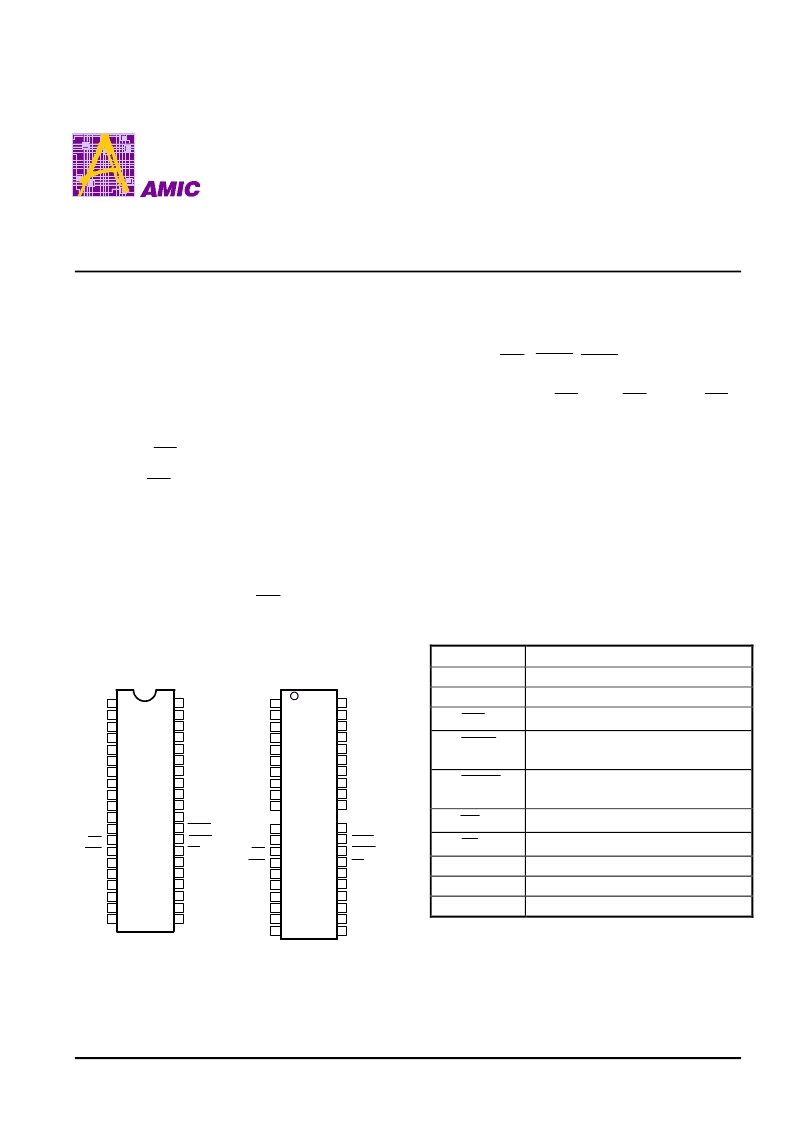
Pin Configuration
n
SOJ
n
TSOP
VCC
I/O
0
I/O
1
I/O
2
I/O
3
VCC
NC
NC
A1
A2
A3
VCC
A4
VSS
A5
A6
A7
A8
I/O
13
I/O
12
VSS
I/O
14
I/O
15
VSS
A
21
WE
RAS
NC
OE
I/O
4
I/O
5
I/O
6
I/O
7
A0
UCAS
LCAS
NC
I/O
8
I/O
9
I/O
10
I/O
11
20
19
18
12
13
14
15
16
17
11
10
9
8
7
6
5
4
3
2
1
22
23
24
25
26
27
28
29
30
31
32
33
34
35
36
37
38
39
40
VCC
I/O
0
I/O
1
I/O
2
I/O
3
VCC
NC
NC
A1
A2
A3
A4
VSS
A5
A6
A7
A8
I/O
13
I/O
12
VSS
I/O
14
I/O
15
VSS
A
23
WE
RAS
NC
I/O
4
I/O
5
I/O
6
I/O
7
A0
UCAS
OE
LCAS
NC
I/O
8
I/O
9
I/O
10
I/O
11
22
21
20
14
15
16
17
18
19
13
10
9
8
7
6
5
4
3
2
1
24
25
26
27
28
29
30
31
32
35
36
37
38
39
40
41
42
43
44
VCC
cycle with a feature called Extended Data Out (FAST).
This allow random access of up to 512 words within a row
at a 66/52 MHz FAST cycle, making the A418316 ideally
suited for graphics, digital signal processing and high
performance computing systems.
Pin Descriptions
Symbol
Description
A0 – A8
I/O
0
- I/O
15
Address Inputs
Data Input/Output
Row Address Strobe
RAS
LCAS
Column Address Strobe for Lower Byte
(I/O
0
– I/O
7
)
Column Address Strobe for Upper Byte
(I/O
8
– I/O
15
)
Write Enable
UCAS
WE
OE
Output Enable
VCC
VSS
NC
5.0V Power Supply
Ground
No Connection
相關(guān)PDF資料 |
PDF描述 |
|---|---|
| A418316V-35 | 256K X 16 CMOS DYNAMIC RAM WITH FAST PAGE MODE |
| A418316V-35U | 256K X 16 CMOS DYNAMIC RAM WITH FAST PAGE MODE |
| A418316S | 256K X 16 CMOS DYNAMIC RAM WITH FAST PAGE MODE |
| A418316 | 256K X 16 CMOS DYNAMIC RAM WITH FAST PAGE MODE |
| A418316V | 256K X 16 CMOS DYNAMIC RAM WITH FAST PAGE MODE |
相關(guān)代理商/技術(shù)參數(shù) |
參數(shù)描述 |
|---|---|
| A418316V-35 | 制造商:AMICC 制造商全稱:AMIC Technology 功能描述:256K X 16 CMOS DYNAMIC RAM WITH FAST PAGE MODE |
| A418316V-35U | 制造商:AMICC 制造商全稱:AMIC Technology 功能描述:256K X 16 CMOS DYNAMIC RAM WITH FAST PAGE MODE |
| A4184-02 | 制造商:HAMAMATSU 制造商全稱:Hamamatsu Corporation 功能描述:Housings, Power and Signal Cables, Connector Adapters |
| A4184-03 | 制造商:HAMAMATSU 制造商全稱:Hamamatsu Corporation 功能描述:Housings, Power and Signal Cables, Connector Adapters |
| A-418A | 制造商:DWYER INSTRUMENTS 功能描述:A-418A ASSY PRESS SNSR WALL MT |
發(fā)布緊急采購,3分鐘左右您將得到回復(fù)。