- 您現(xiàn)在的位置:買賣IC網(wǎng) > PDF目錄92885 > A19-1 10 MHz - 1000 MHz RF/MICROWAVE WIDE BAND MEDIUM POWER AMPLIFIER PDF資料下載
參數(shù)資料
| 型號: | A19-1 |
| 元件分類: | 放大器 |
| 英文描述: | 10 MHz - 1000 MHz RF/MICROWAVE WIDE BAND MEDIUM POWER AMPLIFIER |
| 封裝: | TO-8, 4 PIN |
| 文件頁數(shù): | 1/2頁 |
| 文件大小: | 361K |
| 代理商: | A19-1 |
Cascadable Amplifier
10 to 1000 MHz
A19-1 / SMA19-1
M/A-COM Inc. and its affiliates reserve the right to make changes to the
product(s) or information contained herein without notice. M/A-COM makes
no warranty, representation or guarantee regarding the suitability of its
products for any particular purpose, nor does M/A-COM assume any liability
whatsoever arising out of the use or application of any product(s) or
information.
North America Tel: 800.366.2266 / Fax: 978.366.2266
Europe Tel: 44.1908.574.200 / Fax: 44.1908.574.300
Asia/Pacific Tel: 81.44.844.8296 / Fax: 81.44.844.8298
Visit www.macom.com for additional data sheets and product information.
V3
1
Electrical Specifications: Z0 = 50
, VCC = +15 VDC
Parameter
Typical
Guaranteed
25C
0 to 50C
-54 to +85C*
Frequency
MHz
10-1100
10-1000
Small Signal Gain (min)
dB
11.5
10.5
10.0
Gain Flatness (max)
dB
±0.2
±0.6
±0.8
Reverse Isolation
dB
16
Noise Figure (max)
dB
5.5
6.5
7.0
Power Output
@ 1 dB comp. (min)
dBm
22.5
20.5
20.0
IP3
dBm
+35
IP2
dBm
+51
Second Order Harmonic IP
dBm
+58
VSWR Input / Output (max)
1.5:1 / 1.5:1
1.7:1 / 1.7:1
2.0:1 / 2.3:1
DC Current @ 15 Volts (max)
mA
90
94
99
Units
Features
HIGH OUTPUT POWER: +22.5 dBm (TYP.)
HIGH THIRD ORDER I.P.: +35 dBm (TYP.)
MEDIUM NOISE FIGURE: 6.0 dB (TYP.)
Description
The A19-1 RF amplifier is a discrete thin film hybrid design,
which incorporates the use of thin film manufacturing processes
for accurate performance and high reliability.
This single stage bipolar transistor feedback amplifier design
displays impressive performance over a broadband frequency
range. An active DC biasing network is used for temperature-
stable performance, in addition to an RF Choke, used for power
supply decoupling.
Both TO-8 and Surface Mount packages are hermetically
sealed, and MIL-STD-883 environmental screening is available
.
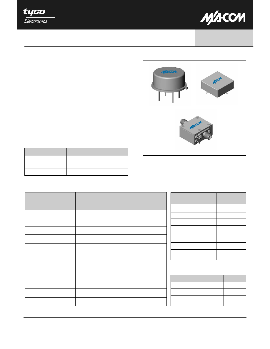
Product Image
Ordering Information
Part Number
Package
A19-1
TO-8
SMA19-1
Surface Mount
CA19-1
SMA Connectorized
Absolute Maximum Ratings
Parameter
Absolute
Maximum
Storage Temperature
-62C to +125C
Case Temperature
+125C
DC Voltage
+17 V
Continuous Input Power
+13 dBm
Short Term Input power
(1 minute max.)
100 mW
Peak Power (3 sec max.)
0.5 W
“S” Series Burn-In
Temperature (case)
+125C
Thermal Data: VCC = +15 VDC
Parameter
Rating
Thermal Resistance θjc
100C/W
Transistor Power Dissipation Pd
0.907 W
Junction Temperature Rise
Above Case Tjc
+91C
* Over temperature performance limits for part number CA19-1, guaranteed from 0
oC to +50oC only.
相關(guān)PDF資料 |
PDF描述 |
|---|---|
| A19-1 | 10 MHz - 1000 MHz RF/MICROWAVE WIDE BAND MEDIUM POWER AMPLIFIER |
| A1 | 5 MHz - 500 MHz RF/MICROWAVE WIDE BAND LOW POWER AMPLIFIER |
| A2002 | 20 MHz - 2700 MHz RF/MICROWAVE WIDE BAND MEDIUM POWER AMPLIFIER |
| A24 | 5 MHz - 1500 MHz RF/MICROWAVE WIDE BAND LOW POWER AMPLIFIER |
| A24 | 5 MHz - 1500 MHz RF/MICROWAVE WIDE BAND LOW POWER AMPLIFIER |
相關(guān)代理商/技術(shù)參數(shù) |
參數(shù)描述 |
|---|---|
| A191 31M | 制造商:DORMER TOOLS 功能描述:MIN. DRILL BIT SET |
| A19-1_1 | 制造商:MA-COM 制造商全稱:M/A-COM Technology Solutions, Inc. 功能描述:Cascadable Amplifier 10 to 1000 MHz |
| A19105-000 | 制造商:TE Connectivity 功能描述:2424A1631-9 |
| A-19107 | 制造商:LG Corporation 功能描述:CRT AND YOKE ASSEMBLY 32V (VDC |
| A-19111 | 制造商:LG Corporation 功能描述:CRT 32V W DEFLECTIONYOKE |
發(fā)布緊急采購,3分鐘左右您將得到回復。