- 您現(xiàn)在的位置:買賣IC網(wǎng) > PDF目錄4178 > A1440A-1VQG100C (Microsemi SoC)IC FPGA 4K GATES 100-VQFP PDF資料下載
參數(shù)資料
| 型號: | A1440A-1VQG100C |
| 廠商: | Microsemi SoC |
| 文件頁數(shù): | 41/90頁 |
| 文件大小: | 0K |
| 描述: | IC FPGA 4K GATES 100-VQFP |
| 產(chǎn)品變化通告: | A1440A Family Discontinuation 24/Jan/2012 |
| 標(biāo)準(zhǔn)包裝: | 90 |
| 系列: | ACT™ 3 |
| LAB/CLB數(shù): | 564 |
| 輸入/輸出數(shù): | 83 |
| 門數(shù): | 4000 |
| 電源電壓: | 4.5 V ~ 5.5 V |
| 安裝類型: | 表面貼裝 |
| 工作溫度: | 0°C ~ 70°C |
| 封裝/外殼: | 100-TQFP |
| 供應(yīng)商設(shè)備封裝: | 100-VQFP(14x14) |
第1頁第2頁第3頁第4頁第5頁第6頁第7頁第8頁第9頁第10頁第11頁第12頁第13頁第14頁第15頁第16頁第17頁第18頁第19頁第20頁第21頁第22頁第23頁第24頁第25頁第26頁第27頁第28頁第29頁第30頁第31頁第32頁第33頁第34頁第35頁第36頁第37頁第38頁第39頁第40頁當(dāng)前第41頁第42頁第43頁第44頁第45頁第46頁第47頁第48頁第49頁第50頁第51頁第52頁第53頁第54頁第55頁第56頁第57頁第58頁第59頁第60頁第61頁第62頁第63頁第64頁第65頁第66頁第67頁第68頁第69頁第70頁第71頁第72頁第73頁第74頁第75頁第76頁第77頁第78頁第79頁第80頁第81頁第82頁第83頁第84頁第85頁第86頁第87頁第88頁第89頁第90頁
Detailed Specifications
2- 38
R e visio n 3
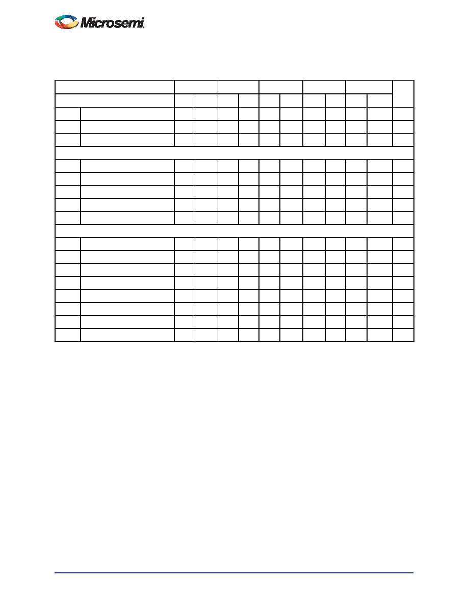
A14100A, A14V100A Timing Characteristics
Table 2-34 A14100A, A14V100A Worst-Case Commercial Conditions, VCC = 4.75 V, TJ = 70°C
1
Logic Module Propagation Delays2
–3 Speed3
–2 Speed 3
–1 Speed
Std. Speed
3.3 V Speed1 Units
Parameter/Description
Min.
Max.
Min. Max. Min.
Max.
Min.
Max.
Min.
Max.
tPD
Internal Array Module
2.0
2.3
2.6
3.0
3.9
ns
tCO
Sequential Clock to Q
2.0
2.3
2.6
3.0
3.9
ns
tCLR
Asynchronous Clear to Q
2.0
2.3
2.6
3.0
3.9
ns
Predicted Routing Delays4
tRD1
FO = 1 Routing Delay
0.9
1.0
1.1
1.3
1.7
ns
tRD2
FO = 2 Routing Delay
1.2
1.4
1.6
1.8
2.4
ns
tRD3
FO = 3 Routing Delay
1.4
1.6
1.8
2.1
2.8
ns
tRD4
FO = 4 Routing Delay
1.7
1.9
2.2
2.5
3.3
ns
tRD8
FO = 8 Routing Delay
2.8
3.2
3.6
4.2
5.5
ns
Logic Module Sequential Timing
tSUD
Flip-Flop Data Input Setup
0.5
0.6
0.8
ns
tHD
Flip-Flop Data Input Hold
0.0
0.5
ns
tSUD
Latch Data Input Setup
0.5
0.6
0.8
ns
tHD
Latch Data Input Hold
0.0
0.5
ns
tWASYN Asynchronous Pulse Width
2.4
3.2
3.8
4.8
6.5
ns
tWCLKA Flip-Flop Clock Pulse Width
2.4
3.2
3.8
4.8
6.5
ns
tA
Flip-Flop Clock Input Period
5.0
6.8
8.0
10.0
13.4
ns
fMAX
Flip-Flop Clock Frequency
200
150
125
100
75
MHz
Notes:
1. VCC = 3.0 V for 3.3 V specifications.
2. For dual-module macros, use tPD + tRD1 + tPDn + tCO + tRD1 + tPDn or tPD1 + tRD1 + tSUD, whichever is appropriate.
3. The –2 and –3 speed grades have been discontinued. Refer to PDN 0104, PDN 0203, PDN 0604, and PDN 1004 at
4. Routing delays are for typical designs across worst-case operating conditions. These parameters should be used for
estimating device performance. Post-route timing analysis or simulation is required to determine actual worst-case
performance. Post-route timing is based on actual routing delay measurements performed on the device prior to
shipment.
相關(guān)PDF資料 |
PDF描述 |
|---|---|
| ASC65DRTS | CONN EDGECARD 130PS .100 DIP SLD |
| ASC65DRES | CONN EDGECARD 130POS .100 EYELET |
| A1225A-PQG100I | IC FPGA 2500 GATES 100-PQFP IND |
| AMC36DRYS | CONN EDGECARD 72POS .100 DIP SLD |
| ACB106DHNT-S621 | CONN EDGECARD 212PS .050 DIP SLD |
相關(guān)代理商/技術(shù)參數(shù) |
參數(shù)描述 |
|---|---|
| A1440A-1VQG100I | 功能描述:IC FPGA 4K GATES 100-VQFP RoHS:是 類別:集成電路 (IC) >> 嵌入式 - FPGA(現(xiàn)場可編程門陣列) 系列:ACT™ 3 產(chǎn)品變化通告:XC4000(E,L) Discontinuation 01/April/2002 標(biāo)準(zhǔn)包裝:24 系列:XC4000E/X LAB/CLB數(shù):100 邏輯元件/單元數(shù):238 RAM 位總計:3200 輸入/輸出數(shù):80 門數(shù):3000 電源電壓:4.5 V ~ 5.5 V 安裝類型:表面貼裝 工作溫度:-40°C ~ 100°C 封裝/外殼:120-BCBGA 供應(yīng)商設(shè)備封裝:120-CPGA(34.55x34.55) |
| A1440A-2PG175C | 制造商:未知廠家 制造商全稱:未知廠家 功能描述:Field Programmable Gate Array (FPGA) |
| A1440A-2PL84C | 制造商:Microsemi Corporation 功能描述:FPGA ACT 3 4K GATES 564 CELLS 200MHZ 0.8UM 5V 84PLCC - Rail/Tube 制造商:Microsemi SOC Products Group 功能描述:FPGA ACT 3 4K GATES 564 CELLS 200MHZ 0.8UM 5V 84PLCC - Rail/Tube |
| A1440A-2PL84I | 制造商:Microsemi SOC Products Group 功能描述:FPGA ACT 3 4K GATES 564 CELLS 200MHZ 0.8UM 5V 84PLCC - Rail/Tube |
| A1440A-2PLG84C | 制造商:Microsemi Corporation 功能描述:FPGA ACT 3 4K GATES 564 CELLS 200MHZ 0.8UM 5V 84PLCC - Rail/Tube 制造商:Microsemi SOC Products Group 功能描述:FPGA ACT 3 4K GATES 564 CELLS 200MHZ 0.8UM 5V 84PLCC - Rail/Tube |
發(fā)布緊急采購,3分鐘左右您將得到回復(fù)。