- 您現(xiàn)在的位置:買賣IC網(wǎng) > PDF目錄375099 > A1186LUA-T (Allegro MicroSystems, Inc.) Ultrasensitive Two-Wire Field-Programmable Chopper-Stabilized Unipolar Hall-Effect Switches PDF資料下載
參數(shù)資料
| 型號(hào): | A1186LUA-T |
| 廠商: | Allegro MicroSystems, Inc. |
| 英文描述: | Ultrasensitive Two-Wire Field-Programmable Chopper-Stabilized Unipolar Hall-Effect Switches |
| 中文描述: | 超靈敏雙線現(xiàn)場(chǎng)可編程斬波穩(wěn)定單極霍爾效應(yīng)開(kāi)關(guān) |
| 文件頁(yè)數(shù): | 3/14頁(yè) |
| 文件大小: | 318K |
| 代理商: | A1186LUA-T |
第1頁(yè)第2頁(yè)當(dāng)前第3頁(yè)第4頁(yè)第5頁(yè)第6頁(yè)第7頁(yè)第8頁(yè)第9頁(yè)第10頁(yè)第11頁(yè)第12頁(yè)第13頁(yè)第14頁(yè)
3
A1185-DS, Rev. 1
Worcester, Massachusetts 01615-0036 (508) 853-5000
www.allegromicro.com
115 Northeast Cutoff, Box 15036
Allegro MicroSystems, Inc.
Ultrasensitive Two-Wire Field-Programmable Chopper-Stabilized Unipolar Hall Effect Switches
A1185 and A1186
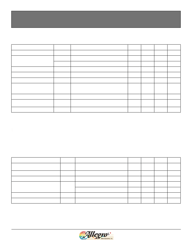
ELECTRICAL CHARACTERISTICS
over the operating voltage and temperature ranges, unless otherwise specified
Characteristic
Symbol
Test Conditions
Min.
Typ.
Max.
Units
Supply Voltage
1
V
CC
Device powered on
3.5
–
24
V
Supply Current
2
I
CC(L)
B >B
OP
for A1185; B <B
RP
for A1186
5
–
6.9
mA
I
CC(H)
B >B
OP
for A1186; B <B
RP
for A1185
12
–
17
mA
Supply Zener Clamp Voltage
V
ZSupply
I
CC
= I
CC(L)(Max)
+ 3 mA; T
A
= 25°C
28
–
40
V
Supply Zener Clamp Current
3
I
ZSupply
V
Supply
= 28 V
–
–
9.9
mA
Reverse Supply Current
I
RCC
V
RCC
= –18 V
No bypass capacitor; capacitance of the
oscilloscope performing the measurement
= 20 pF
–
–
1.6
mA
Output Slew Rate
4
di/dt
–
36
–
mA/
μ
s
Chopping Frequency
f
C
–
200
–
kHz
Power-On Time
5
t
on
After factory trimming; with and without
bypass capacitor (C
BYP
= 0.01
μ
F)
t
on
≤
t
on(max)
;
V
CC
slew rate > 25 mV/
μ
s
–
–
25
μ
s
Power-On State
6,7
POS
–
HIGH
–
–
1
V
CC
represents the generated voltage between the VCC pin and the GND pin.
2
Relative values of B use the algebraic convention, where positive values indicate south magnetic polarity, and negative values indicate north magnetic
polarity; therefore greater B values indicate a stronger south polarity field (or a weaker north polarity field, if present).
3
I
ZSUPPLY(max)
= I
CCL(max)
+ 3 mA.
4
Measured without bypass capacitor between VCC and GND. Use of a bypass capacitor results in slower current change.
5
Measured with and without bypass capacitor of 0.01
μ
F. Adding a larger bypass capacitor causes longer Power-On Time.
6
POS is defined as true only with a V
CC
slew rate of 25 mV /
μ
s or greater. Operation with a V
CC
slew rate less than 25 mV /
μ
s can permanently harm
device performance.
7
POS is undefined for t > t
on
or B
RP
< B < B
OP
.
MAGNETIC CHARACTERISTICS
1
over the operating voltage and temperature ranges, unless otherwise specified
Characteristic
Symbol
Test Conditions
Min.
Typ.
Max.
Units
Programmable Operate Point Range
B
OPrange
I
CC
= I
CC(L)
for A1185
I
CC
= I
CC(H)
for A1186
V
CC
= 12 V
10
–
60
G
Initial Operate Point Range
B
OPinit
–
–10
10
G
Switchpoint Step Size
2
B
RES
V
CC
= 5 V, T
A
= 25°C
2
4
6
G
Number of Programming Bits
–
Switchpoint setting
–
5
–
Bit
Programming locking
–
1
–
Bit
Temperature Drift of B
OP
Δ
B
OP
–
–
±20
G
Hysteresis
B
HYS
B
HYS
= B
OP
– B
RP
5
15
30
G
1
Relative values of B use the algebraic convention, where positive values indicate south magnetic polarity, and negative values indicate north magnetic
polarity; therefore greater B values indicate a stronger south polarity field (or a weaker north polarity field, if present).
2
The range of values specified for B
RES
is a maximum, derived from the cumulative programming bit errors.
相關(guān)PDF資料 |
PDF描述 |
|---|---|
| A1186LLHLT | Ultrasensitive Two-Wire Field-Programmable Chopper-Stabilized Unipolar Hall-Effect Switches |
| A1185 | Ultrasensitive Two-Wire Field-Programmable Chopper-Stabilized Unipolar Hall-Effect Switches |
| A1185EUA-T | Ultrasensitive Two-Wire Field-Programmable Chopper-Stabilized Unipolar Hall-Effect Switches |
| A1185LLHLT-T | Ultrasensitive Two-Wire Field-Programmable Chopper-Stabilized Unipolar Hall-Effect Switches |
| A1185LUA | RES MF 24.3K OHM 1%0.250W@ 70C 100PPM/TC AXL |
相關(guān)代理商/技術(shù)參數(shù) |
參數(shù)描述 |
|---|---|
| A1187 | 制造商:Quick 功能描述:TSOJ 18.5mm x 8mm Nozzle for 21-13205 and 21-13210 制造商:QUICK 功能描述:TSOJ 18.5 X 8 NOZZLE FOR QUICK957/957D |
| A1-18-701-15 | 制造商:Southco 功能描述: |
| A118734 | 制造商:SRC Devices 功能描述: 制造商:Coto Technology 功能描述: |
| A1188 | 制造商:Quick 功能描述:PLCC 9 X 9 NOZZLE FOR QUICK957/957D |
| A1189 | 制造商:Quick 功能描述:PLCC 34mm X 34mm Nozzle for 21-13205 and 21-13210 制造商:QUICK 功能描述:PLCC 34 X 34 NOZZLE FOR QUICK957/957D 制造商:HAKKO Corporation 功能描述: |
發(fā)布緊急采購(gòu),3分鐘左右您將得到回復(fù)。