- 您現(xiàn)在的位置:買賣IC網(wǎng) > PDF目錄375097 > A1141LLH (Allegro MicroSystems, Inc.) Sensitive Two-Wire Chopper-Stabilized Unipolar Hall-Effect Switches PDF資料下載
參數(shù)資料
| 型號: | A1141LLH |
| 廠商: | Allegro MicroSystems, Inc. |
| 英文描述: | Sensitive Two-Wire Chopper-Stabilized Unipolar Hall-Effect Switches |
| 中文描述: | 敏感的兩線斬波穩(wěn)定單極霍爾效應(yīng)開關(guān) |
| 文件頁數(shù): | 3/11頁 |
| 文件大?。?/td> | 393K |
| 代理商: | A1141LLH |
3
A1140-DS
Worcester, Massachusetts 01615-0036 (508) 853-5000
www.allegromicro.com
115 Northeast Cutoff, Box 15036
Allegro MicroSystems, Inc.
Sensitive Two-Wire Chopper-Stabilized Unipolar Hall Effect Switches
A1140/41/42/43
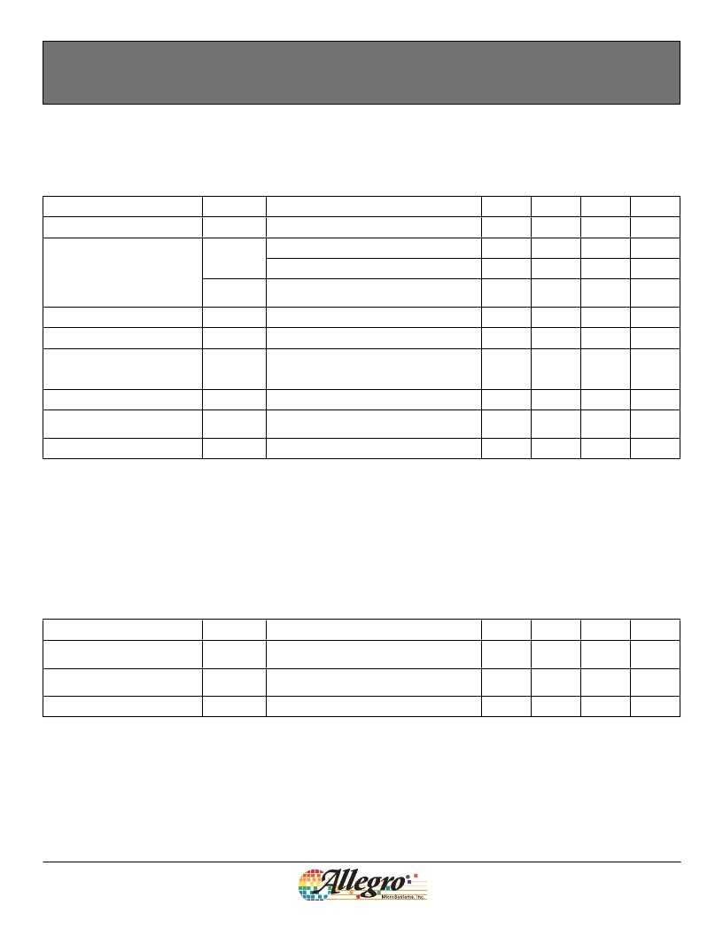
ELECTRICAL CHARACTERISTICS
over the operating voltage and temperature range, unless otherwise speci
fi
ed
Characteristic
Symbol
Test Conditions
Min.
Typ.
Max.
Units
Supply Voltage
V
CC
Device powered on
3.5
–
24
V
Supply Current
1
I
CC(L)
B >B
OP
for A1140; B <B
RP
for A1141
2
–
5
mA
B >B
OP
for A1142; B <B
RP
for A1143
B >B
OP
for A1141, A1143
B <B
RP
for A1140, A1142
I
CC
= I
CC(max)
+ 3 mA; T
A
= 25°C
5
–
6.9
mA
I
CC(H)
12
–
17
mA
Zener Clamp Supply Voltage
V
Z(supply)
28
–
40
V
Zener Clamp Supply Current
2
I
Z(supply)
V
Z(supply)
= 28 V
No bypass capacitor; capacitance of the
oscilloscope performing the measurement
= 20 pF
–
–
10
mA
Output Slew Rate
3
di/dt
–
36
–
mA/μs
Chopping Frequency
f
C
–
400
–
kHz
Power-On Time
4
t
on
After factory programming; with and without
bypass capacitor (C
BYP
= 0.01 μF)
t
on
≤
t
on(max)
;
V
CC
slew rate
≥
25 mV/
μ
s
–
–
25
μ
s
Power-On State
5
POS
–
HIGH
–
–
1
Relative values of B use the algebraic convention, where positive values indicate south magnetic polarity, and negative values indicate north magnetic
polarity; therefore greater B values indicate a stronger south polarity
fi
eld (or a weaker north polarity
fi
eld, if present).
2
The maximum value for I
Z(supply)
is equal to I
CC(L)MAX
+ 3 mA.
3
The value of di is the difference between 90% of I
CC(H)
and 10% of I
CC(L)
, and the value of dt is time period between those two points. The value of di/dt
depends on the value of the bypass capacitor, if one is used, with greater capacitances resulting in lower rates of change.
4
The value of t
on
depends on the value of the bypass capacitor, if one is used, with greater capacitances resulting in longer t
on
.
5
A V
CC
slew rate less than 25 mV/
μ
s affects device performance, both while powering-on and while running. For t
on
> t
on(max)
, and B
RP
< B < B
OP
, POS
is unde
fi
ned.
MAGNETIC CHARACTERISTICS*
over the operating voltage and temperature range, unless otherwise speci
fi
ed
Characteristic
Symbol
Test Conditions
Min.
Typ.
Max.
Units
Operate Point
B
OP
I
CC(H)
→
I
CC(L)
for A1140, A1142
I
CC(L)
→
I
CC(H)
for A1141, A1143
I
CC(L)
→
I
CC(H)
for A1140, A1142
I
CC(H)
→
I
CC(L)
for A1141, A1143
B
HYS
= B
OP
– B
RP
50
85
115
G
Release Point
B
RP
45
–
110
G
Hysteresis
B
HYS
5
15
30
G
*Relative values of B use the algebraic convention, where positive values indicate south magnetic polarity, and negative values indicate north magnetic
polarity; therefore greater B values indicate a stronger south polarity
fi
eld (or a weaker north polarity
fi
eld, if present).
相關(guān)PDF資料 |
PDF描述 |
|---|---|
| A1142LUA | Sensitive Two-Wire Chopper-Stabilized Unipolar Hall-Effect Switches |
| A1143ELH | Sensitive Two-Wire Chopper-Stabilized Unipolar Hall-Effect Switches |
| A1140EUATI-T4 | Sensitive Two-Wire Chopper-Stabilized Unipolar Hall Effect Switches |
| A1140LUATI-T4 | Sensitive Two-Wire Chopper-Stabilized Unipolar Hall Effect Switches |
| A1141 | Sensitive Two-Wire Chopper-Stabilized Unipolar Hall Effect Switches |
相關(guān)代理商/技術(shù)參數(shù) |
參數(shù)描述 |
|---|---|
| A1141LUA | 制造商:ALLEGRO 制造商全稱:Allegro MicroSystems 功能描述:Sensitive Two-Wire Chopper-Stabilized Unipolar Hall-Effect Switches |
| A1141LUATI-T4 | 制造商:ALLEGRO 制造商全稱:Allegro MicroSystems 功能描述:Sensitive Two-Wire Chopper-Stabilized Unipolar Hall Effect Switches |
| A1141U2N2NZNQ | 功能描述:旋鈕開關(guān) SP 90 DEG. 2 POS RoHS:否 制造商:C&K Components 位置數(shù)量:5 卡片組數(shù)量: 每卡片組極數(shù):2 電流額定值:250 mA 電壓額定值:125 V 指數(shù)角: 觸點(diǎn)類型: 觸點(diǎn)形式:DPST 端接類型:Solder 安裝類型:Panel 觸點(diǎn)電鍍:Silver |
| A1142 | 制造商:HAKKO Corporation 功能描述: |
| A11421100 | 制造商:LAMB INDUSTRIES 功能描述: |
發(fā)布緊急采購,3分鐘左右您將得到回復(fù)。