- 您現(xiàn)在的位置:買賣IC網(wǎng) > PDF目錄25516 > 954204AGT (INTEGRATED DEVICE TECHNOLOGY INC) 400 MHz, PROC SPECIFIC CLOCK GENERATOR, PDSO56 PDF資料下載
參數(shù)資料
| 型號: | 954204AGT |
| 廠商: | INTEGRATED DEVICE TECHNOLOGY INC |
| 元件分類: | 時鐘產生/分配 |
| 英文描述: | 400 MHz, PROC SPECIFIC CLOCK GENERATOR, PDSO56 |
| 封裝: | 6.10 MM, 0.50 MM PITCH, MO-153, TSSOP-56 |
| 文件頁數(shù): | 12/20頁 |
| 文件大小: | 261K |
| 代理商: | 954204AGT |
2
Integrated
Circuit
Systems, Inc.
ICS954204
0933D—03/16/05
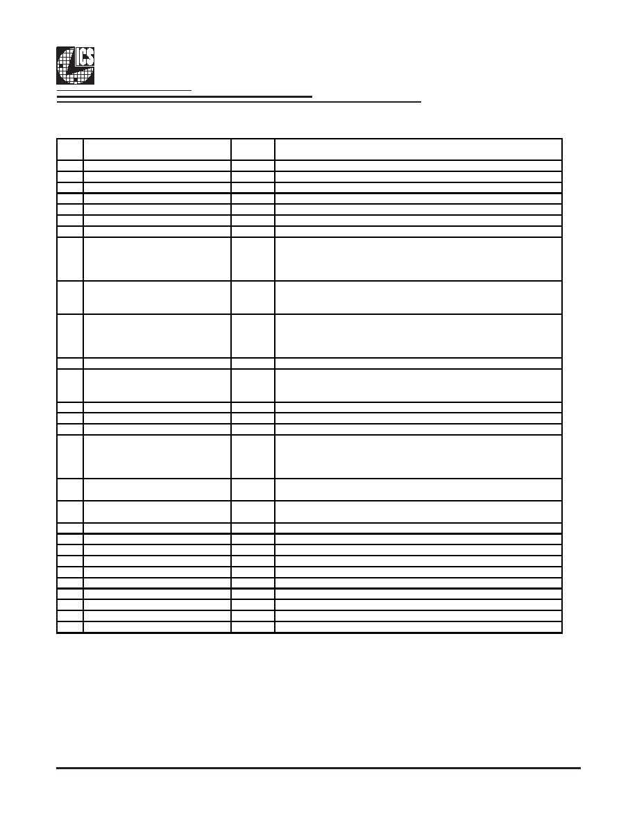
Pin Description
PIN # PIN NAME
PIN TYPE DESCRIPTION
1
VDDPCI
PWR
Power supply for PCI clocks, nominal 3.3V
2
GND
PWR
Ground pin.
3
PCICLK3
OUT
PCI clock output.
4
PCICLK4
OUT
PCI clock output.
5
PCICLK5
OUT
PCI clock output.
6
GND
PWR
Ground pin.
7
VDDPCI
PWR
Power supply for PCI clocks, nominal 3.3V
8
ITP_EN/PCICLK_F0
I/O
Free running PCI clock not affected by PCI_STOP#.
ITP_EN: latched input to select pin functionality
1 = CPU_ITP pair
0 = SRC pair
9
*SELSRC_LCDCLK#/PCICLK_F1
I/O
Latched input select for LCD_ss/ SRCCLK output frequency:
0 = LCD,
1 = SRCCLK/ 3.3V free-running PCI clock output.
10
Vtt_PwrGd#/PD
IN
Vtt_PwrGd# is an active low input used to determine when latched inputs
are ready to be sampled. PD is an asynchronous active high input pin used
to put the device into a low power state. The internal clocks, PLLs and the
crystal oscillator are stopped.
11
VDD48
PWR
Power pin for the 48MHz output.3.3V
12
FSLA/USB_48MHz
I/O
3.3V tolerant input for CPU frequency selection. Refer to input electrical
characteristics for Vil_FS and Vih_FS values. / Fixed 48MHz USB clock
output. 3.3V.
13
GND
PWR
Ground pin.
14
DOTT_96MHz
OUT
True clock of differential pair for 96.00MHz DOT clock.
15
DOTC_96MHz
OUT
Complement clock of differential pair for 96.00MHz DOT clock.
16
FSLB/TEST_MODE
IN
3.3V tolerant input for CPU frequency selection. Refer to input electrical
characteristics for Vil_FS and Vih_FS values. TEST_MODE is a real time
input to select between Hi-Z and REF/N divider mode while in test mode.
Refer to Test Clarification Table.
17
LCDCLK_SST/SRCCLKT0
OUT
True clock of LCDCLK_SS output / True clock of SRCCLK differential pair.
Selected by SEL_LCDCLK#
18
LCDCLK_SSC/SRCCLKC0
OUT
Complementary clock of LCDCLK_SS output / Complementary clock of
SRCCLK differential pair. Selected by SEL_LCDCLK#
19
SRCCLKT1
OUT
True clock of differential SRC clock pair.
20
SRCCLKC1
OUT
Complement clock of differential SRC clock pair.
21
VDDSRC
PWR
Supply for SRC clocks, 3.3V nominal
22
SRCCLKT2
OUT
True clock of differential SRC clock pair.
23
SRCCLKC2
OUT
Complement clock of differential SRC clock pair.
24
SRCCLKT3
OUT
True clock of differential SRC clock pair.
25
SRCCLKC3
OUT
Complement clock of differential SRC clock pair.
26
SRCCLKT4_SATA
OUT
True clock of differential SRC/SATA pair.
27
SRCCLKC4_SATA
OUT
Complement clock of differential SRC/SATA pair.
28
VDDSRC
PWR
Supply for SRC clocks, 3.3V nominal
相關PDF資料 |
PDF描述 |
|---|---|
| 954206BGT | 400 MHz, PROC SPECIFIC CLOCK GENERATOR, PDSO56 |
| 954206BFT | 400 MHz, PROC SPECIFIC CLOCK GENERATOR, PDSO56 |
| 954206BFLFT | 400 MHz, PROC SPECIFIC CLOCK GENERATOR, PDSO56 |
| 9552-6006-01 | RF/MICROWAVE FIXED ATTENUATOR |
| 9552-6006-03 | RF/MICROWAVE FIXED ATTENUATOR |
相關代理商/技術參數(shù) |
參數(shù)描述 |
|---|---|
| 954204BGLF | 制造商:Integrated Device Technology Inc 功能描述:56 TSSOP (LEAD FREE) - Rail/Tube |
| 954204BGLN | 制造商:Integrated Device Technology Inc 功能描述:PLL Clock Synthesizer Dual 56-Pin TSSOP Tube |
| 954204BGLNT | 制造商:Integrated Device Technology Inc 功能描述:PLL Clock Synthesizer Dual 56-Pin TSSOP T/R |
| 954204CGLF | 功能描述:時鐘合成器/抖動清除器 RoHS:否 制造商:Skyworks Solutions, Inc. 輸出端數(shù)量: 輸出電平: 最大輸出頻率: 輸入電平: 最大輸入頻率:6.1 GHz 電源電壓-最大:3.3 V 電源電壓-最小:2.7 V 封裝 / 箱體:TSSOP-28 封裝:Reel |
| 954204CGLFT | 功能描述:時鐘合成器/抖動清除器 RoHS:否 制造商:Skyworks Solutions, Inc. 輸出端數(shù)量: 輸出電平: 最大輸出頻率: 輸入電平: 最大輸入頻率:6.1 GHz 電源電壓-最大:3.3 V 電源電壓-最小:2.7 V 封裝 / 箱體:TSSOP-28 封裝:Reel |
發(fā)布緊急采購,3分鐘左右您將得到回復。