- 您現(xiàn)在的位置:買賣IC網(wǎng) > PDF目錄24864 > 950902DGLFT (INTEGRATED DEVICE TECHNOLOGY INC) 200.4 MHz, PROC SPECIFIC CLOCK GENERATOR, PDSO56 PDF資料下載
參數(shù)資料
| 型號(hào): | 950902DGLFT |
| 廠商: | INTEGRATED DEVICE TECHNOLOGY INC |
| 元件分類: | 時(shí)鐘產(chǎn)生/分配 |
| 英文描述: | 200.4 MHz, PROC SPECIFIC CLOCK GENERATOR, PDSO56 |
| 封裝: | 6.10 MM, 0.50 MM PITCH, MO-153, TSSOP-56 |
| 文件頁數(shù): | 16/22頁 |
| 文件大?。?/td> | 210K |
| 代理商: | 950902DGLFT |
3
Integrated
Circuit
Systems, Inc.
ICS950902
0475F—10/13/03
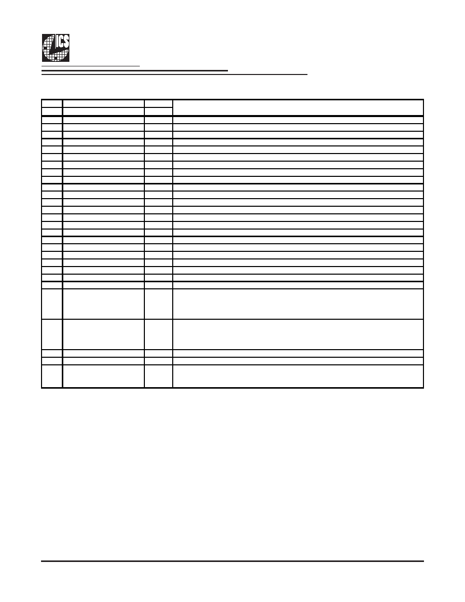
Pin Description Continued
PIN
#
NAME
TYPE
29
DDRC5/SDRAM11
OUT
"Complementary" Clock of differential memory output / 3.3V SDRAM clock output
30
DDRT5/SDRAM10
OUT
"True" Clock of differential memory output / 3.3V SDRAM clock output
31
DDRC4/SDRAM9
OUT
"Complementary" Clock of differential memory output / 3.3V SDRAM clock output
32
DDRT4/SDRAM8
OUT
"True" Clock of differential memory output / 3.3V SDRAM clock output
33
GND
PWR
Ground pin.
34
VDD3.3_2.5
PWR
2.5V or 3.3V nominal power supply voltage.
35
DDRC3/SDRAM7
OUT
"Complementary" Clock of differential memory output / 3.3V SDRAM clock output
36
DDRT3/SDRAM6
OUT
"True" Clock of differential memory output / 3.3V SDRAM clock output
37
DDRC2/SDRAM5
OUT
"Complementary" Clock of differential memory output / 3.3V SDRAM clock output
38
DDRT2/SDRAM4
OUT
"True" Clock of differential memory output / 3.3V SDRAM clock output
39
GND
PWR
Ground pin.
40
VDD3.3_2.5
PWR
2.5V or 3.3V nominal power supply voltage.
41
DDRC1/SDRAM3
OUT
"Complementary" Clock of differential memory output / 3.3V SDRAM clock output
42
DDRT1/SDRAM2
OUT
"True" Clock of differential memory output / 3.3V SDRAM clock output
43
DDRC0/SDRAM1
OUT
"Complementary" Clock of differential memory output / 3.3V SDRAM clock output
44
DDRT0/SDRAM0
OUT
"True" Clock of differential memory output / 3.3V SDRAM clock output
45
BUF_IN
IN
Input Buffers for memory outputs.
46
FBOUT
OUT
Memory feed back output.
47
GND
PWR
Ground pin.
48
CPUT_CS
OUT
"True" clocks of differential pair 2.5V push-pull CPU outputs.
49
CPUC_CS
OUT
Complementary" clocks of differential pair 2.5V push-pull CPU outputs.
50
VDDCPU2.5
PWR
Power pin for the CPUCLKs. 2.5V
51
VDDCPU3.3
PWR
Power pin for the CPUCLKs. 3.3V
52
CPUCLKC/CPUCLKODC
OUT
"Complementary" clocks of differential pair CPU outputs. These are current mode outputs.
External resistors are required for voltage bias / "Complementary" clocks of differential pair
CPU outputs. These open drain outputs need an external 1.5V pull-up / 2.5V CPU clock
output.
53
CPUCLKT/CPUCLKODT
OUT
"True" clocks of differential pair CPU outputs. These are current mode outputs. External
resistors are required for voltage bias / "True" clocks of differential pair CPU outputs. These
open drain outputs need an external 1.5V pull-up / 2.5V CPU clock output.
54
GND
PWR
Ground pin.
55
VDDREF
PWR
Ref, XTAL power supply, nominal 3.3V
56
Vtt_PWRGD#**/REF1
IN
This 3.3V LVTTL input is a level sensitive strobe used to determine when latch inputs are
valid and are ready to be sampled. This is an active low input. / 14.318 MHz reference clock.
DESCRIPTION
相關(guān)PDF資料 |
PDF描述 |
|---|---|
| 08056C103JAT7A | Separating plate, width: 0.8 mm, color: gray - TS-GSK |
| 08056C103JAT9A | General Specifications |
| 950902DGLF | 200.4 MHz, PROC SPECIFIC CLOCK GENERATOR, PDSO56 |
| 08056C103KA72A | General Specifications |
| 950908BGLF | 200.4 MHz, PROC SPECIFIC CLOCK GENERATOR, PDSO56 |
相關(guān)代理商/技術(shù)參數(shù) |
參數(shù)描述 |
|---|---|
| 9509060100 | 制造商:未知廠家 制造商全稱:未知廠家 功能描述:Computer Cable for EIA RS-232 Applications |
| 95090601000 | 制造商:未知廠家 制造商全稱:未知廠家 功能描述:Computer Cable for EIA RS-232 Applications |
| 9509060500 | 制造商:未知廠家 制造商全稱:未知廠家 功能描述:Computer Cable for EIA RS-232 Applications |
| 950-908 | 制造商:Mitutoyo Corporation 功能描述:TOOL KIT, MACHINIST |
| 950908BF | 制造商:Ics 功能描述:200.4 MHz, PROC SPECIFIC CLOCK GENERATOR, 56 Pin Plastic SMT |
發(fā)布緊急采購,3分鐘左右您將得到回復(fù)。