- 您現(xiàn)在的位置:買賣IC網(wǎng) > PDF目錄24864 > 950812YGLFT (INTEGRATED DEVICE TECHNOLOGY INC) 200 MHz, PROC SPECIFIC CLOCK GENERATOR, PDSO56 PDF資料下載
參數(shù)資料
| 型號: | 950812YGLFT |
| 廠商: | INTEGRATED DEVICE TECHNOLOGY INC |
| 元件分類: | 時鐘產(chǎn)生/分配 |
| 英文描述: | 200 MHz, PROC SPECIFIC CLOCK GENERATOR, PDSO56 |
| 封裝: | 6.10 MM, 0.50 MM PITCH, GREEN, MO-153, TSSOP-56 |
| 文件頁數(shù): | 29/30頁 |
| 文件大小: | 227K |
| 代理商: | 950812YGLFT |
第1頁第2頁第3頁第4頁第5頁第6頁第7頁第8頁第9頁第10頁第11頁第12頁第13頁第14頁第15頁第16頁第17頁第18頁第19頁第20頁第21頁第22頁第23頁第24頁第25頁第26頁第27頁第28頁當前第29頁第30頁
IDTTM Frequency Generator with 200MHz Differential CPU Clocks
0542J—01/25/10
ICS950812
Frequency Generator with 200MHz Differential CPU Clocks
8
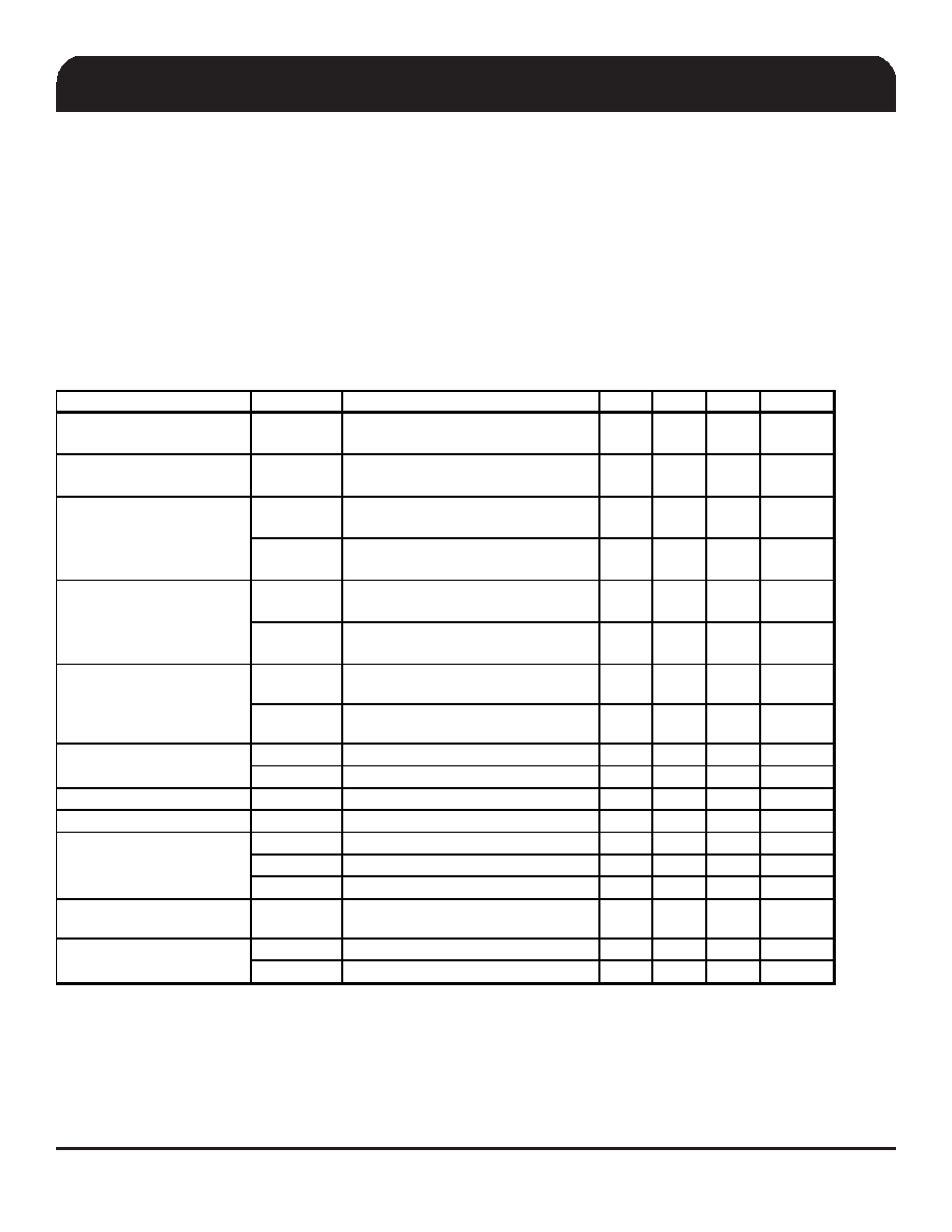
Absolute Maximum Ratings
Supply Voltage
5.5 V
Logic Inputs
GND –0.5 V to VDD +0.5 V
Ambient Operating Temperature
0°C to +90°C
Case Temperature
115°C
Storage Temperature
–65°C to +150°C
Stresses above those listed under
Absolute Maximum Ratings may cause permanent damage to the device. These ratings are
stress specifications only and functional operation of the device at these or any other conditions above those listed in the
operational sections of the specifications is not implied. Exposure to absolute maximum rating conditions for extended
periods may affect product reliability.
Electrical Characteristics - Input/Supply/Common Output Parameters
TA = 0 - 90°C; Supply Voltage VDD = 3.3 V +/-5%
PARAMETER
SYMBOL
CONDITIONS
MIN
TYP
MAX
UNITS
Input High Voltage
VIH
2
VDD+0.
3
V
Input Low Voltage
VIL
VSS-
0.3
0.8
V
IIH
VIN = VDD; Inputs with no pull-down
resistors
5.75
mA
IIH
VIN = VDD; Inputs with pull-down
resistors
200
A
IIL1
VIN = 0 V; Inputs with no pull-up
resistors
-5.75
mA
IIL2
VIN = 0 V; Inputs with pull-up
resistors
-200
A
IDD3.3OP
CL = Full load; Select @ 100 MHz
233
280
mA
IDD3.3OP
CL =Full load; Select @ 133 MHz
234
280
mA
IDD3.3PD
IREF=5 mA
20
52
mA
IDD3.3PDHIz
0.289
0.5
mA
Input Frequency
Fi
VDD = 3.3 V
14.32
MHz
Pin Inductance
Lpin
7nH
CIN
Logic Inputs
5
pF
COUT
Output pin capacitance
6
pF
CINX
X1 & X2 pins
27
30
45
pF
Clk Stabilization
1,2
TSTAB
From PowerUp or deassertion of
PowerDown to 1st clock.
12.1
ms
tPZH,tPZL
Output enable delay (all outputs)
1
12
ns
tPHZ,tPLZ
Output disable delay (all outputs)
1
12
ns
1Guaranteed by design, not 100% tested in production.
2See timing diagrams for buffered and un-buffered timing requirements.
Delay
1
Input Capacitance
1
Input High Current
Input Low Current
Operating Supply Current
Powerdown Current
相關PDF資料 |
PDF描述 |
|---|---|
| 950812YGT | 200 MHz, PROC SPECIFIC CLOCK GENERATOR, PDSO56 |
| 950902DGLFT | 200.4 MHz, PROC SPECIFIC CLOCK GENERATOR, PDSO56 |
| 08056C103JAT7A | Separating plate, width: 0.8 mm, color: gray - TS-GSK |
| 08056C103JAT9A | General Specifications |
| 950902DGLF | 200.4 MHz, PROC SPECIFIC CLOCK GENERATOR, PDSO56 |
相關代理商/技術參數(shù) |
參數(shù)描述 |
|---|---|
| 950813 | 制造商:Weidmuller 功能描述:NEXT 74/55/16, 4GP, ST, ZINC -EA - Bulk |
| 9508131 | 制造商:Molex 功能描述: |
| 9508141 | 制造商:Molex 功能描述:Conn Housing RCP 14 POS 3.96mm Crimp ST Bag |
| 9508143 | 制造商:Molex 功能描述: |
| 950815 | 制造商:Weidmuller 功能描述:NEXT 98/74/16, 4GP, ST, ZINC -EA - Bulk |
發(fā)布緊急采購,3分鐘左右您將得到回復。