- 您現(xiàn)在的位置:買賣IC網(wǎng) > PDF目錄36343 > 935277468118 (NXP SEMICONDUCTORS) 1-CHANNEL, SGL POLE DOUBLE THROW SWITCH, PDSO8 PDF資料下載
參數(shù)資料
| 型號(hào): | 935277468118 |
| 廠商: | NXP SEMICONDUCTORS |
| 元件分類: | 多路復(fù)用及模擬開關(guān) |
| 英文描述: | 1-CHANNEL, SGL POLE DOUBLE THROW SWITCH, PDSO8 |
| 封裝: | SOT-96, ROHS COMPLIANT, PLASTIC, SO-8 |
| 文件頁(yè)數(shù): | 17/20頁(yè) |
| 文件大?。?/td> | 395K |
| 代理商: | 935277468118 |
第1頁(yè)第2頁(yè)第3頁(yè)第4頁(yè)第5頁(yè)第6頁(yè)第7頁(yè)第8頁(yè)第9頁(yè)第10頁(yè)第11頁(yè)第12頁(yè)第13頁(yè)第14頁(yè)第15頁(yè)第16頁(yè)當(dāng)前第17頁(yè)第18頁(yè)第19頁(yè)第20頁(yè)
Philips Semiconductors
Product specification
SA630
Single pole double throw (SPDT) switch
1997 Nov 07
6
The isolation and matching of the two channels over frequency is
shown in Figures 15 and 17, respectively.
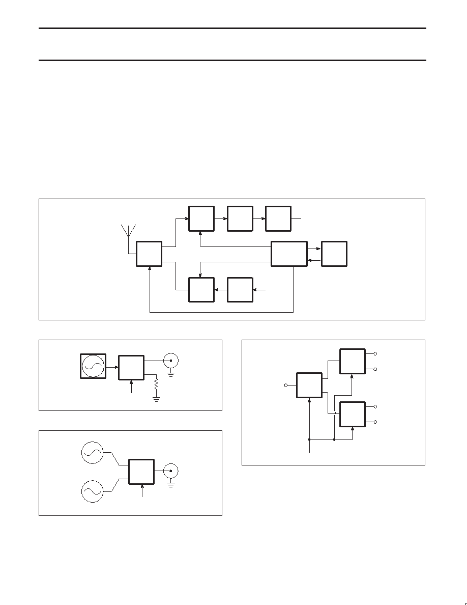
The SA630 is a very versatile part and can be used in many
applications. Figure 5 shows a block diagram of a typical Digital RF
transceiver front-end. In this application the SA630 replaces the
duplexer which is typically very bulky and lossy. Due to the low
power consumption of the device, it is ideally suited for handheld
applications such as in CT2 cordless telephones. The SA630 can
also be used to generate Amplitude Shift Keying (ASK) or On-Off
Keying (OOK) and Frequency Shift Keying (FSK) signals for digital
RF communications systems. Block diagrams for these applications
are shown in Figures 6 and 7, respectively.
For applications that require a higher isolation at 1GHz than
obtained from a single SA630, several SA630s can be cascaded as
shown in Figure 8. The cascaded configuration will have a higher
loss but greater than 35dB of isolation at 1GHz and greater than
65dB @ 500MHz can be obtained from this configuration. By
modifying the enable control, an RF multiplexer/ de-multiplexer or
antenna selector can be constructed. The simplicity of SA630
coupled with its ease of use and high performance lends itself to
many innovative applications.
The SA630 switch terminates the OFF channel in 50
. The 50
resistor is internal and is in series with the external AC bypass
capacitor. Matching to impedances other than 50
can be achieved
by adding a resistor in series with the AC bypass capacitor (e.g.,
25
additional to match to a 75 environment).
5200
630
MODULATION
602A
IF OUT
5200
VCO
MICRO
Tx/Rx
KEYPAD
&
DISPLAY
CONTROLLER
SR00582
Figure 5. A Typical TDMA/Digital RF Transceiver System Front-End
630
ASK OUTPUT
ENABLE
CH1
OSCILLATOR
TTL DATA
50
SR00583
Figure 6. Amplitude Shift Keying (ASK) Generator
630
FSK OUTPUT
ENABLE
CH1
TTL DATA
f1
f2
SR00584
Figure 7. Frequency Shift Keying (FSK) Gnerator
630
IN/OUT
630
OUT1/IN1
OUT2/IN2
ENABLE
SR00585
Figure 8.
相關(guān)PDF資料 |
PDF描述 |
|---|---|
| 935052500602 | 1-CHANNEL, SGL POLE DOUBLE THROW SWITCH, PDSO8 |
| 935052500118 | 1-CHANNEL, SGL POLE DOUBLE THROW SWITCH, PDSO8 |
| 935278155557 | SPECIALTY CONSUMER CIRCUIT, PBGA456 |
| 935278338557 | SPECIALTY CONSUMER CIRCUIT, PBGA456 |
| 935279245557 | SPECIALTY CONSUMER CIRCUIT, PBGA456 |
相關(guān)代理商/技術(shù)參數(shù) |
參數(shù)描述 |
|---|---|
| 935277864112 | 制造商:NXP Semiconductors 功能描述:IC CPU |
| 935278818112 | 制造商:NXP Semiconductors 功能描述:LCD DRVR 20DIGIT 2.5V/3.3V/5V 56-Pin VSO Tube |
| 935280517132 | 制造商:NXP Semiconductors 功能描述:IC TRANSLATING BUFFER 6XSON |
| 935281751112 | 制造商:NXP Semiconductors 功能描述:IC BUFFER/DVR 16BIT 3ST 48TSSOP |
| 935281751118 | 制造商:NXP Semiconductors 功能描述:IC BUFFER/DVR 16BIT 3ST 48TSSOP |
發(fā)布緊急采購(gòu),3分鐘左右您將得到回復(fù)。