- 您現(xiàn)在的位置:買賣IC網(wǎng) > PDF目錄36341 > 935270968115 (NXP SEMICONDUCTORS) 1-CHANNEL POWER SUPPLY SUPPORT CKT, PDSO5 PDF資料下載
參數(shù)資料
| 型號(hào): | 935270968115 |
| 廠商: | NXP SEMICONDUCTORS |
| 元件分類: | 電源管理 |
| 英文描述: | 1-CHANNEL POWER SUPPLY SUPPORT CKT, PDSO5 |
| 封裝: | 1.50 MM, PLASTIC, MO-178, SOT-23, SO-5 |
| 文件頁(yè)數(shù): | 13/15頁(yè) |
| 文件大小: | 197K |
| 代理商: | 935270968115 |
第1頁(yè)第2頁(yè)第3頁(yè)第4頁(yè)第5頁(yè)第6頁(yè)第7頁(yè)第8頁(yè)第9頁(yè)第10頁(yè)第11頁(yè)第12頁(yè)當(dāng)前第13頁(yè)第14頁(yè)第15頁(yè)
Philips Semiconductors
Product data
NE56631-XX
Active-LOW system reset
2003 Feb 14
7
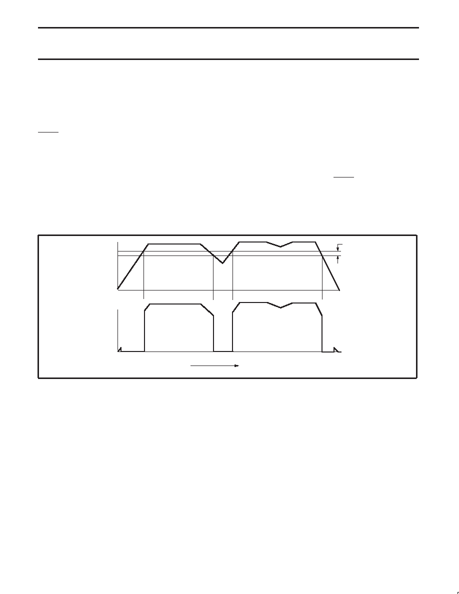
TIMING DIAGRAM
The Timing Diagram in Figure 10 depicts the operation of the device.
Letters A–J on the Time axis indicates specific events.
A:
At “A”, VCC begins to increase. Also the VOUT voltage initially
increases but abruptly decreases when VCC reaches the level
(approximately 0.65 V) that activates the internal bias circuitry and
RESET is asserted.
B:
At “B”, VCC reaches the threshold level of VSH. At this point the
device releases the hold on the VOUT reset. The Reset output VOUT
tracks VCC as it rises above VSH (assuming the reset pull-up resistor
RPU is connected to VCC). In a microprocessor-based system these
events release the reset from the microprocessor, allowing the
microprocessor to function normally.
C-D:
At “C”, VCC begins to fall, causing VOUT to follow. VCC
continues to fall until the VSL undervoltage detection threshold is
reached at “D”. This causes a reset signal to be generated (VOUT
RESET goes LOW).
D-E:
Between “D” and “E”, VCC starts rising.
E:
At “E”, VCC rises to the VSH level. Once again, the device
releases the hold on the VOUT reset. The Reset output tracks VCC
as it rises above VSH.
F-G:
At “F”, VCC is above the upper threshold and begins to fall,
causing VOUT to follow it. As long as VCC remains above the VSH,
no reset signal will be triggered. Before VCC falls to the VSH, it
begins to rise, causing VOUT to follow it. At “G”, VCC returns to
normal.
H:
At event “H”, VCC falls until the VSL undervoltage detection
threshold is reached. At this level, a RESET signal is generated and
VOUT goes LOW.
J:
At “J”, the VCC voltage has decreased until normal internal
circuit bias is unable to maintain a VOUT reset. As a result, VCC may
rise to less than 0.65 V. As VCC decreases further, the VOUT reset
also decreases to zero.
SL01740
VCC
VOUT
TIME
VSH
VSL
0
AB
C
G
H
J
DE
F
VS
Figure 10. Timing diagram.
相關(guān)PDF資料 |
PDF描述 |
|---|---|
| 935270975115 | 1-CHANNEL POWER SUPPLY SUPPORT CKT, PDSO5 |
| 935270977115 | 1-CHANNEL POWER SUPPLY SUPPORT CKT, PDSO5 |
| 935270971115 | 1-CHANNEL POWER SUPPLY SUPPORT CKT, PDSO5 |
| 935270974115 | 1-CHANNEL POWER SUPPLY SUPPORT CKT, PDSO5 |
| 935270993115 | 1-CHANNEL POWER SUPPLY SUPPORT CKT, PDSO5 |
相關(guān)代理商/技術(shù)參數(shù) |
參數(shù)描述 |
|---|---|
| 935271394518 | 制造商:NXP Semiconductors 功能描述:IC MCU ARM 20TSSOP |
| 935271933518 | 制造商:NXP Semiconductors 功能描述:IC D-TYPE POS TRG DUAL 56VFBGA |
| 935271933551 | 制造商:NXP Semiconductors 功能描述:IC D-TYPE POS TRG DUAL 56VFBGA |
| 935271933557 | 制造商:NXP Semiconductors 功能描述:IC D-TYPE POS TRG DUAL 56VFBGA |
| 935271937518 | 制造商:NXP Semiconductors 功能描述:IC BUFF DVR TRI-ST 16BIT 56VFBGA |
發(fā)布緊急采購(gòu),3分鐘左右您將得到回復(fù)。