- 您現(xiàn)在的位置:買賣IC網(wǎng) > PDF目錄36341 > 935270466518 (NXP SEMICONDUCTORS) 2-CHANNEL POWER SUPPLY SUPPORT CKT, PDSO8 PDF資料下載
參數(shù)資料
| 型號: | 935270466518 |
| 廠商: | NXP SEMICONDUCTORS |
| 元件分類: | 電源管理 |
| 英文描述: | 2-CHANNEL POWER SUPPLY SUPPORT CKT, PDSO8 |
| 封裝: | 4.40 MM, PLASTIC, SOT-530-1, VSOP-8 |
| 文件頁數(shù): | 5/10頁 |
| 文件大?。?/td> | 131K |
| 代理商: | 935270466518 |
Philips Semiconductors
Product data
NE57607
Two-cell Lithium-ion battery protection with
overcurrent, over- and under-voltage protection
2001 Oct 03
4
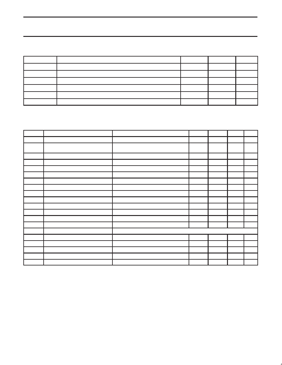
MAXIMUM RATINGS
SYMBOL
PARAMETER
Min.
Max.
UNIT
VIN(max)
Input voltage
–0.3
+18
V
VCF(max)
Maximum CF pin voltage
–
VIN–0.6
V
VCS(max)
Maximum CS pin voltage
–
VIN–0.6
V
Topr
Operating ambient temperature range
–20
+70
°C
Tstg
Storage temperature
–40
+125
°C
PD
Power dissipation
–
300
mW
ELECTRICAL CHARACTERISTICS
Tamb = 25 °C; VCEL = V4–V3 = V3–V2 = V2–V1 = V1–GND; VCC = 4VCEL, except where noted otherwise.
SYMBOL
PARAMETER
CONDITIONS
Min.
Typ.
Max.
UNIT
VOC
Overcharge detection voltage
Tamb = 0 °C 50 °C
4.325
4.350
4.375
V
VOC
Overcharge detection hysteresis
voltage
170
220
270
mV
VOD
Overdischarge detection voltage
2.20
2.30
2.40
V
IVC2(1)
Consumption current 1
VC2 = VC1 = 1.0 V; VCS = 1.4 V
–
0.1
A
IVC2(2)
Consumption current 2
VC2 = VC1 = 1.9 V; VCS = 3.2 V
–
0.5
0.8
A
IVC23
Consumption current 3
VC2 = VC1 = 3.5 V
–
15.0
20.0
A
IVC24
Consumption current 4
VC2 = VC1 = 4.5 V; ROC = 270 k
–
150
A
IVC1
VC1 pin input current
VC2 = VC1 = 3.5 V
–0.3
0
0.3
A
VDF
Overdischarge release voltage
Discharge resume by voltage rise
3.30
3.50
3.70
V
VGDH
GD pin HIGH output voltage
VC2 = VC1 = 3.5 V; IL = –10 A
VC2–0.3
VC2–0.2
–
V
VGDL
GD pin LOW output voltage
VC2 = VC1 = 3.5 V; IL = 10 A
–
0.2
0.3
V
ICFH
CF pin output current
VC2 = VC1 = 4.5 V
–
30
150
A
VCS1
Overcurrent detection threshold value
135
150
165
mV
VCS2
Short circuit threshold value
When both battery pack pins are shorted
0.35
0.45
0.55
V
Overcurrent release
Load release: Load of 5MEG
& or more between both battery pack pins
tOC1
Overcurrent detection delay time 1
7
12
18
ms
tOC2
Overcurrent detection delay time 2
Note 1
–
30
100
s
tOD
Overdischarge detection delay time
8
13
20
ms
tOCH
Overcharge detection dead time
CDLY = 0.18 F; Note 2
0.5
1.0
1.5
s
VST
Start-up voltage
VC2 = VC1 = 2.5 V
–0.24
–0.12
–0.04
V
NOTES:
1. The short-circuit delay time is for the IC only. This time will increase with the discharge FET gate capacitance. The short-circuit condition
may cause the cell voltage to collapse and lengthen the delay.
2. Calculate overcharge dead time according to the following formula:
Talm – 5.55 × CTD
(time expressed in seconds, capacitance in
F)
相關(guān)PDF資料 |
PDF描述 |
|---|---|
| 935270462518 | 2-CHANNEL POWER SUPPLY SUPPORT CKT, PDSO8 |
| 935270464518 | 2-CHANNEL POWER SUPPLY SUPPORT CKT, PDSO8 |
| 935270461518 | 2-CHANNEL POWER SUPPLY SUPPORT CKT, PDSO8 |
| 935270463518 | 2-CHANNEL POWER SUPPLY SUPPORT CKT, PDSO8 |
| 935270476115 | 1-CHANNEL POWER SUPPLY SUPPORT CKT, PDSO6 |
相關(guān)代理商/技術(shù)參數(shù) |
參數(shù)描述 |
|---|---|
| 935270713557 | 制造商:NXP Semiconductors 功能描述:SUB ONLY IC CHP |
| 935270792551 | 制造商:NXP Semiconductors 功能描述:IC BUFF DVR TRI-ST 16BIT 56VFBGA |
| 935270792557 | 制造商:NXP Semiconductors 功能描述:IC BUFF DVR TRI-ST 16BIT 56VFBGA |
| 935270793551 | 制造商:NXP Semiconductors 功能描述:IC BUS TRCVR 3-ST 16BIT 56VFBGA |
| 935270793557 | 制造商:NXP Semiconductors 功能描述:IC BUS TRCVR 3-ST 16BIT 56VFBGA |
發(fā)布緊急采購,3分鐘左右您將得到回復(fù)。