- 您現(xiàn)在的位置:買賣IC網(wǎng) > PDF目錄76381 > 935269817112 (NXP SEMICONDUCTORS) LOW SKEW CLOCK DRIVER, 10 TRUE OUTPUT(S), 0 INVERTED OUTPUT(S), PDSO28 PDF資料下載
參數(shù)資料
| 型號: | 935269817112 |
| 廠商: | NXP SEMICONDUCTORS |
| 元件分類: | 時鐘及定時 |
| 英文描述: | LOW SKEW CLOCK DRIVER, 10 TRUE OUTPUT(S), 0 INVERTED OUTPUT(S), PDSO28 |
| 封裝: | 5.30 MM, PLASTIC, MO-150, SOT-341-1, SSOP-28 |
| 文件頁數(shù): | 9/12頁 |
| 文件大小: | 92K |
| 代理商: | 935269817112 |
Philips Semiconductors
Product data
PCK2002M
0–300 MHz I2C 1:10 clock buffer
2001 Jul 19
6
I2C CONSIDERATIONS
I2C has been chosen as the serial bus interface to control the PCK2001M. I2C was chosen to support the JEDEC proposal JC-42.5 168-Pin
Unbuffered SDRAM DIMM. All vendors are required to determine the legal issues associated with the manufacture of I2C devices.
1) Address assignment: The clock driver in this specification uses the single, 7-bit address shown below. All devices can use the address if only
one master clock driver is used in a design. The address can be re-used for the CKBF device if no other conflicting I2C clock driver is used in
the system.
The following address was confirmed by Philips on 09/04/96.
A6
A5
A4
A3
A2
A1
A0
R/W
11
01
00
10
NOTE: The R/W bit is used by the I2C controller as a data direction bit. A ‘zero’ indicates a transmission (WRITE) to the clock device. A ‘one’
indicates a request for data (READ) from the clock driver. Since the definition of the clock buffer only allows the controller to WRITE data; the
R/W bit of the address will always be seen as ‘zero’. Optimal address decoding of this bit is left to the vendor.
2) Options: It is our understanding that metal mask options and other pinouts of this type of clock driver will be allowed to use the same address
as the original CKBF device. I2C addresses are defined in terms of function (master clock driver) rather than form (pinout, and option).
3) Slave/Receiver: The clock driver is assumed to require only slave/receiver functionality. Slave/transmitter functionality is optional.
4) Data Transfer Rate: 100 kbits/s (standard mode) is the base functionality required. Fast mode (400 kbits/s) functionality is optional.
5) Logic Levels: I2C logic levels are based on a percentage of VDD for the controller and other devices on the bus. Assume all devices are
based on a 3.3 Volt supply.
6) Data Byte Format: Byte format is 8 Bits as described in the following appendices.
7) Data Protocol: To simplify the clock I2C interface, the clock driver serial protocol was specified to use only block writes from the controller.
The bytes must be accessed in sequential order from lowest to highest byte with the ability to stop after any complete byte has been
transferred. Indexed bytes are not allowed. However, the SMBus controller has a more specific format than the generic I2C protocol.
The clock driver must meet this protocol which is more rigorous than previously stated I2C protocol. Treat the description from the viewpoint of
controller. The controller “writes” to the clock driver and if possible would ‘‘read” from the clock driver (the clock driver is a slave/receiver only
and is incapable of this transaction.)
“The block write begins with a slave address and a write condition. After the command code the host (controller) issues a byte count which
describes how many more bytes will follow in the message. If the host had 20 bytes to send, the first byte would be the number 20 (14h),
followed by the 20 bytes of data. The byte count may not be 0. A block write command is allowed to transfer a maximum of 32 data bytes.”
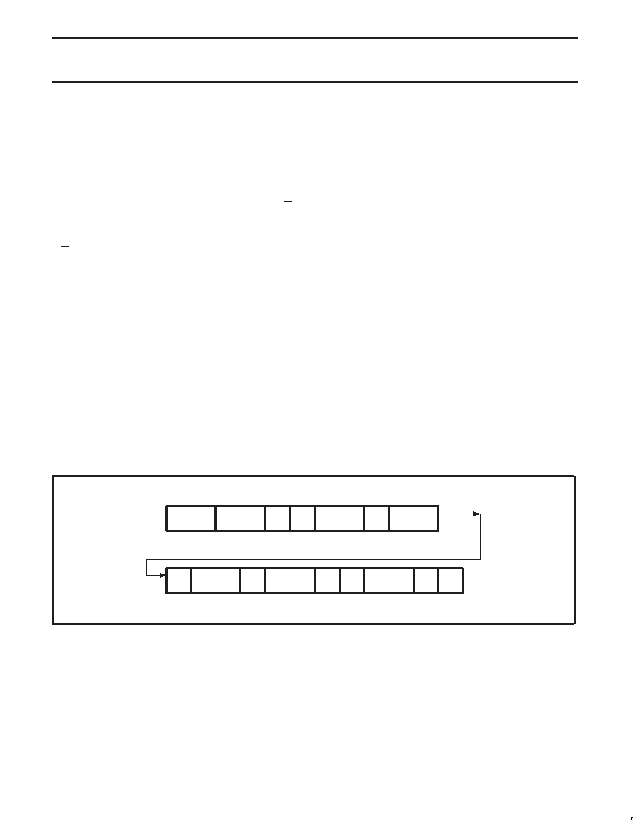
SW00279
1 bit
7 bits
1
8 bits
1
Start bit
Slave Address
R/W
Command Code
Byte Count = N
Ack
Data Byte 1
Ack
Data Byte 2
Ack
...
Data Byte 2
Ack
Stop
Ack
1 bit
8 bits
1
8 bits
1
8 bits
1
NOTE: The acknowledgement bit is returned by the slave/receiver (the clock driver).
Consider the command code and the byte count bytes required as the first two bytes of any transfer. The command code is software
programmable via the controller, but will be specified as 0000 0000 in the clock specification. The byte count byte is the number of additional
bytes required to transfer, not counting the command code and byte count bytes. Additionally, the byte count byte is required to be a minimum of
1 byte and a maximum of 32 bytes to satisfy the above requirement.
相關(guān)PDF資料 |
PDF描述 |
|---|---|
| 935208720118 | ABT SERIES, QUAD 2-INPUT OR GATE, PDSO14 |
| 935269711118 | ALVC/VCX/A SERIES, QUAD 2-INPUT NAND GATE, PDSO14 |
| 935188460118 | HC/UH SERIES, DUAL 4-INPUT NOR GATE, PDSO14 |
| 935189280112 | HCT SERIES, TRIPLE 3-INPUT NOR GATE, PDSO14 |
| 935265465112 | AHC SERIES, 8-BIT RIGHT SERIAL IN PARALLEL OUT SHIFT REGISTER, TRUE OUTPUT, PDSO14 |
相關(guān)代理商/技術(shù)參數(shù) |
參數(shù)描述 |
|---|---|
| 935269987557 | 制造商:NXP Semiconductors 功能描述:SUB ONLY TDA9587-1US1-V1.8 SUBBED TO 935269987557 |
| 935270713557 | 制造商:NXP Semiconductors 功能描述:SUB ONLY IC CHP |
| 935270792551 | 制造商:NXP Semiconductors 功能描述:IC BUFF DVR TRI-ST 16BIT 56VFBGA |
| 935270792557 | 制造商:NXP Semiconductors 功能描述:IC BUFF DVR TRI-ST 16BIT 56VFBGA |
| 935270793551 | 制造商:NXP Semiconductors 功能描述:IC BUS TRCVR 3-ST 16BIT 56VFBGA |
發(fā)布緊急采購,3分鐘左右您將得到回復(fù)。