- 您現(xiàn)在的位置:買賣IC網 > PDF目錄36339 > 935269145115 (NXP SEMICONDUCTORS) 1-CHANNEL POWER SUPPLY SUPPORT CKT, PDSO5 PDF資料下載
參數(shù)資料
| 型號: | 935269145115 |
| 廠商: | NXP SEMICONDUCTORS |
| 元件分類: | 電源管理 |
| 英文描述: | 1-CHANNEL POWER SUPPLY SUPPORT CKT, PDSO5 |
| 封裝: | PLASTIC, SOT-23, SO-5 |
| 文件頁數(shù): | 8/14頁 |
| 文件大小: | 157K |
| 代理商: | 935269145115 |
Philips Semiconductors
Product data
NE56610/11/12-XX
System reset
2001 Jun 19
3
ORDERING INFORMATION
TYPE NUMBER
PACKAGE
TEMPERATURE
TYPICAL
TYPE NUMBER
NAME
DESCRIPTION
RANGE
RESET DELAY
NE56610-XXGW
SOT23-5, SOT25, SO5
plastic small outline package; 5 leads
(see dimensional drawing)
–20 to +75
°C
50 ms
NE56611-XXGW
SOT23-5, SOT25, SO5
plastic small outline package; 5 leads
(see dimensional drawing)
–20 to +75
°C
100 ms
NE56612-XXGW
SOT23-5, SOT25, SO5
plastic small outline package; 5 leads
(see dimensional drawing)
–20 to +75
°C
200 ms
NOTE:
Each device has six detection voltage options, indicated by the XX on the ‘Type number’.
XX
DETECT VOLTAGE (Typical)
25
2.5 V
27
2.7 V
29
2.9 V
39
3.9 V
42
4.2 V
45
4.5 V
Part number marking
Each device is marked with a four letter code. The first three letters designate the product. The fourth letter, represented by ‘x’, is a date tracking
code. For example, ACNB is device ACN (the NE56610-25 reset) produced in time period ‘B’.
Part number
Marking
Part number
Marking
Part number
Marking
NE56610-25
A C N x
NE56611-25
A C V x
NE56612-25
A C B x
NE56610-27
A C M x
NE56611-27
A C U x
NE56612-27
A C A x
NE56610-29
A C L x
NE56611-29
A C T x
NE56612-29
A C Z x
NE56610-39
A C K x
NE56611-39
A C S x
NE56612-39
A C Y x
NE56610-42
A C J x
NE56611-42
A C R x
NE56612-42
A C X x
NE56610-45
A C H x
NE56611-45
A C P x
NE56612-45
A C W x
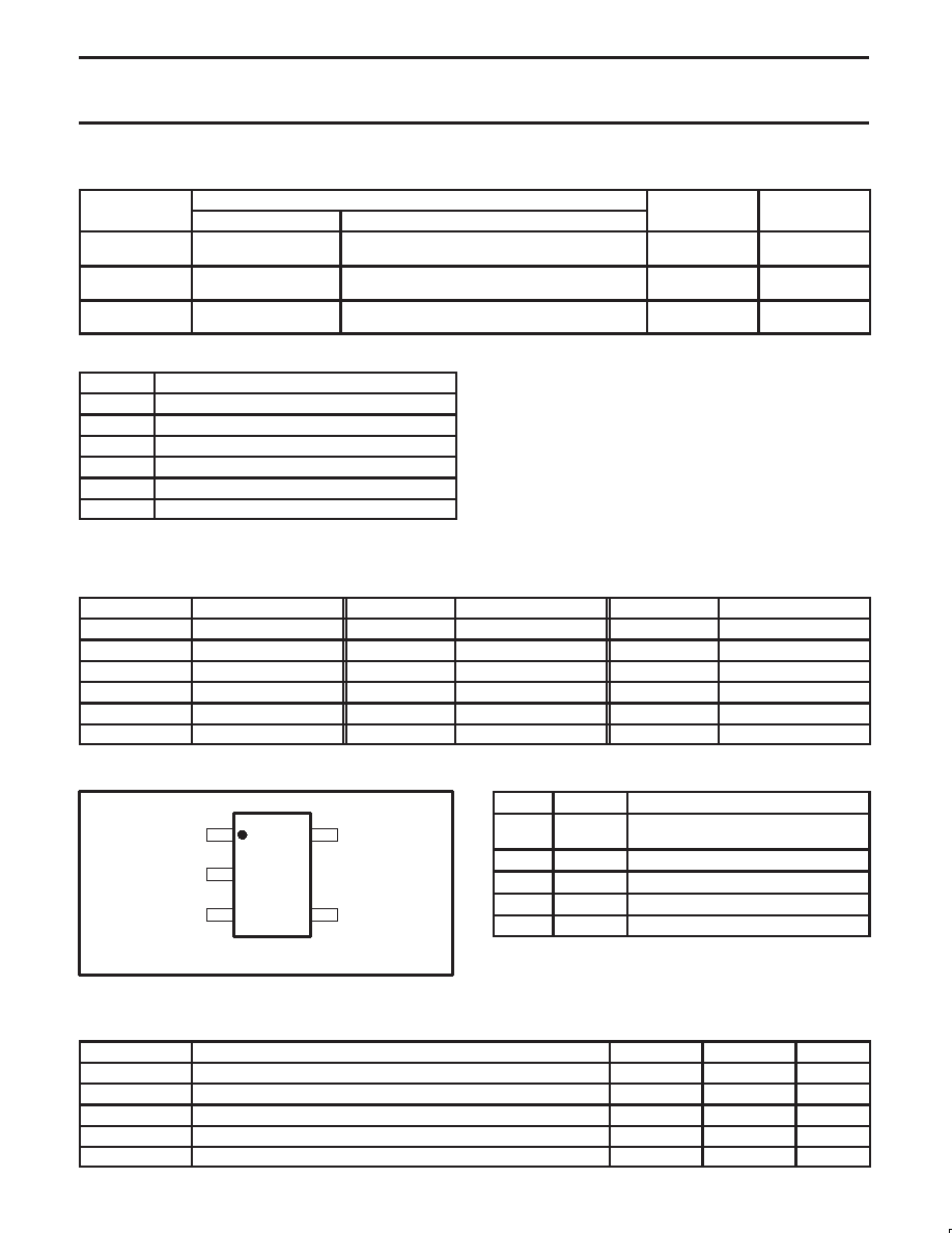
PIN CONFIGURATION
SL01361
1
2
34
5VCC
VOUT
GND
SUB
M/R
NE56610-XX
NE56611-XX
NE56612-XX
Figure 2. Pin configuration.
PIN DESCRIPTION
PIN
SYMBOL
DESCRIPTION
1
M/R
Manual Reset input.
Connect to ground when not using.
2
SUB
Substrate pin. Connect to ground.
3
GND
Ground
4
VOUT
Reset HIGH output pin
5
VCC
Positive power supply input
MAXIMUM RATINGS
SYMBOL
PARAMETER
MIN.
MAX.
UNIT
VCC
Power supply voltage
–0.3
12
V
VM/R
Manual Reset input voltage
–0.3
12
V
Tamb
Operating ambient temperature
–20
75
°C
Tstg
Storage temperature
–40
125
°C
P
Power dissipation
–
150
mW
相關PDF資料 |
PDF描述 |
|---|---|
| 935269179115 | 1-CHANNEL POWER SUPPLY SUPPORT CKT, PDSO5 |
| 935269167115 | 1-CHANNEL POWER SUPPLY SUPPORT CKT, PDSO5 |
| 935269160115 | 1-CHANNEL POWER SUPPLY SUPPORT CKT, PDSO5 |
| 935269156115 | 1-CHANNEL POWER SUPPLY SUPPORT CKT, PDSO5 |
| 935269159115 | 1-CHANNEL POWER SUPPLY SUPPORT CKT, PDSO5 |
相關代理商/技術參數(shù) |
參數(shù)描述 |
|---|---|
| 935269304128 | 制造商:ST-Ericsson 功能描述:IC AUDIO CODEC W/TCH SCRN 48LQFP |
| 935269544557 | 制造商:NXP Semiconductors 功能描述:SUB ONLY TDA9587-2US1-V1.3 |
| 935269987557 | 制造商:NXP Semiconductors 功能描述:SUB ONLY TDA9587-1US1-V1.8 SUBBED TO 935269987557 |
| 935270713557 | 制造商:NXP Semiconductors 功能描述:SUB ONLY IC CHP |
| 935270792551 | 制造商:NXP Semiconductors 功能描述:IC BUFF DVR TRI-ST 16BIT 56VFBGA |
發(fā)布緊急采購,3分鐘左右您將得到回復。