- 您現(xiàn)在的位置:買賣IC網(wǎng) > PDF目錄24805 > 935263530118 (NXP SEMICONDUCTORS) SPECIALTY TELECOM CIRCUIT, PDSO16 PDF資料下載
參數(shù)資料
| 型號: | 935263530118 |
| 廠商: | NXP SEMICONDUCTORS |
| 元件分類: | 通信及網(wǎng)絡(luò) |
| 英文描述: | SPECIALTY TELECOM CIRCUIT, PDSO16 |
| 封裝: | PLASTIC, SOT-403, TSSOP-16 |
| 文件頁數(shù): | 26/31頁 |
| 文件大小: | 224K |
| 代理商: | 935263530118 |
第1頁第2頁第3頁第4頁第5頁第6頁第7頁第8頁第9頁第10頁第11頁第12頁第13頁第14頁第15頁第16頁第17頁第18頁第19頁第20頁第21頁第22頁第23頁第24頁第25頁當(dāng)前第26頁第27頁第28頁第29頁第30頁第31頁
1999 Nov 03
4
Philips Semiconductors
Product specication
SDH/SONET STM4/OC12 and
1.25 Gbits/s Gigabit Ethernet postampliers
TZA3044; TZA3044B
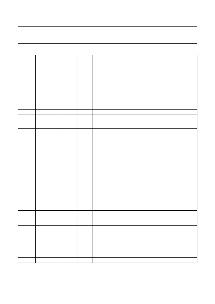
PINNING
Note
1. Pin type abbreviations: O = Output, I = Input, S = power Supply and A = Analog function.
SYMBOL
PIN
TZA3044T
TZA3044TT
PAD
TZA3044U
TYPE(1)
DESCRIPTION
SUB
1
1, 14
S
substrate pin; must be at the same potential as pin AGND
TEST
2
2, 10, 15,
21, 26
for test purpose only; to be left open in the application
AGND
3
3, 4, 6, 9
S
analog ground; must be at the same potential as pin DGND
DIN
4
I
differential input; complementary to pin DINQ; DC bias level is set
internally at approximately 2.1 V
DINQ
5
8
I
differential input; complementary to pin DIN; DC bias level is set
internally at approximately 2.1 V
VCCA
6
11, 12
S
analog supply voltage; must be at the same potential as pin VCCD
CF
7
13
A
input for connection of capacitor to set time constant of level
detector input lter (optional); the capacitor should be connected
between VCCA and pin CF
JAM
8
16
I
PECL-compatible input (TTL compatible for the TZA3044B);
controls the output buffers pins DOUT and DOUTQ; when a LOW
signal is applied, the outputs will follow the input signal; when a
HIGH signal is applied, the output buffers will latch into LOW and
HIGH states respectively; when not connected, pin JAM is actively
pulled LOW
STQ
9
17
O
PECL-compatible status output of the input signal level detector
(TTL compatible for the TZA3044B); when the input signal is below
the user-programmed threshold level, this output is HIGH;
complementary to pin ST
ST
10
18
O
PECL-compatible status output of the input signal level detector
(TTL compatible for the TZA3044B); when the input signal is below
the user-programmed threshold level, this output is LOW;
complementary to pin STQ
DGND
11
19, 20, 22,
25
S
digital ground; must be at the same potential as pin AGND
DOUTQ
12
23
O
PECL-compatible differential output; forced into a HIGH condition
when pin JAM is HIGH; complementary to pin DOUT
DOUT
13
24
O
PECL-compatible differential output; forced into a LOW condition
when pin JAM is HIGH; complementary to pin DOUTQ
VCCD
14
27, 28
S
digital supply voltage; must be at the same potential as VCCA
Vref
15
29
O
band gap reference voltage; typical value is 1.2 V; internal series
resistor of 1 k
RSET
16
30
A
input signal level detector programming; nominal DC voltage is
VCCA 1.5 V; threshold level is set by connecting an external
resistor between VCCA and pin RSET or by forcing a current into
pin RSET; default value for this resistor is 180 k
which
corresponds with approximately 4 mV (p-p) differential input signal
n.c.
5, 31, 32
not connected
相關(guān)PDF資料 |
PDF描述 |
|---|---|
| 935266809025 | SPECIALTY TELECOM CIRCUIT, UUC29 |
| 935266810026 | SPECIALTY TELECOM CIRCUIT, UUC29 |
| 935266812112 | SPECIALTY TELECOM CIRCUIT, PDSO16 |
| 935266812118 | SPECIALTY TELECOM CIRCUIT, PDSO16 |
| 935266813112 | SPECIALTY TELECOM CIRCUIT, PDSO16 |
相關(guān)代理商/技術(shù)參數(shù) |
參數(shù)描述 |
|---|---|
| 935264217557 | 制造商:NXP Semiconductors 功能描述:SUB ONLY IC |
| 935267356112 | 制造商:NXP Semiconductors 功能描述:IC TEA1507PN |
| 935268081112 | 制造商:NXP Semiconductors 功能描述:SUB ONLY IC |
| 935268721125 | 制造商:NXP Semiconductors 功能描述:Buffer/Line Driver 1-CH Non-Inverting 3-ST CMOS 5-Pin TSSOP T/R |
| 935269304128 | 制造商:ST-Ericsson 功能描述:IC AUDIO CODEC W/TCH SCRN 48LQFP |
發(fā)布緊急采購,3分鐘左右您將得到回復(fù)。