- 您現(xiàn)在的位置:買賣IC網(wǎng) > PDF目錄36334 > 935260698551 (NXP SEMICONDUCTORS) SPECIALTY CONSUMER CIRCUIT, PQFP160 PDF資料下載
參數(shù)資料
| 型號: | 935260698551 |
| 廠商: | NXP SEMICONDUCTORS |
| 元件分類: | 消費家電 |
| 英文描述: | SPECIALTY CONSUMER CIRCUIT, PQFP160 |
| 封裝: | PLASTIC, SOT-322, QFP-160 |
| 文件頁數(shù): | 63/148頁 |
| 文件大小: | 692K |
| 代理商: | 935260698551 |
第1頁第2頁第3頁第4頁第5頁第6頁第7頁第8頁第9頁第10頁第11頁第12頁第13頁第14頁第15頁第16頁第17頁第18頁第19頁第20頁第21頁第22頁第23頁第24頁第25頁第26頁第27頁第28頁第29頁第30頁第31頁第32頁第33頁第34頁第35頁第36頁第37頁第38頁第39頁第40頁第41頁第42頁第43頁第44頁第45頁第46頁第47頁第48頁第49頁第50頁第51頁第52頁第53頁第54頁第55頁第56頁第57頁第58頁第59頁第60頁第61頁第62頁當(dāng)前第63頁第64頁第65頁第66頁第67頁第68頁第69頁第70頁第71頁第72頁第73頁第74頁第75頁第76頁第77頁第78頁第79頁第80頁第81頁第82頁第83頁第84頁第85頁第86頁第87頁第88頁第89頁第90頁第91頁第92頁第93頁第94頁第95頁第96頁第97頁第98頁第99頁第100頁第101頁第102頁第103頁第104頁第105頁第106頁第107頁第108頁第109頁第110頁第111頁第112頁第113頁第114頁第115頁第116頁第117頁第118頁第119頁第120頁第121頁第122頁第123頁第124頁第125頁第126頁第127頁第128頁第129頁第130頁第131頁第132頁第133頁第134頁第135頁第136頁第137頁第138頁第139頁第140頁第141頁第142頁第143頁第144頁第145頁第146頁第147頁第148頁
1998 Apr 09
21
Philips Semiconductors
Product specication
Multimedia bridge, high performance
Scaler and PCI circuit (SPCI)
SAA7146A
7.2.2
VIDEO DMA CONTROL
The SAA7146A’s DMA control is able to support up to
three independent video targets or sources respectively.
For this purpose it provides three video DMA channels.
Each channel consists of a FIFO, a FIFO Input Control
(FINC) placed on the video side of the FIFO, and a FIFO
Control (FICO) placed on the PCI side of the FIFO.
Channel 1 only supports the unidirectional data stream
into the PCI memory. It is not able to read data from
system memory. However, this access is possible using
Channels 2 or 3. Table 2 surveys the possibilities and
purposes of each video DMA channel.
Each FIFO, i.e. each DMA channel, has its own
programming set including base address (doubled for odd
and even fields), pitch, protection address, page table
base address, several handling mode control bits and a
transfer enable bit (TR_E). In addition, each channel has a
threshold and a burst length definition for internal
arbitration (see Table 6, Section 7.2.5).
To handle the reading modes FIFO 2 and FIFO 3 offer
some additional registers: Number of Bytes per line
(NumBytes), Number of Lines per field (NumLines) and
the vertical scaling ratio (only FIFO 3, see Table 69).
The programming sets could be reloaded after the
previous job is done [Video Transfer Done (VTD)] to
support several DMA targets per FIFO. The programming
set currently used is loaded by the Register Programming
Sequencer (RPS). If the RPS is not used, the registers
could be rewritten each time, using the SAA7146A as a
slave. But then the programmer must take care of the
synchronization of these write accesses.
All registers needed for DMA control are described in
Table 3, except the transfer enable bits, which are
described in Table 10. The registers are accessed through
PCI base address with appropriate offset (see Table 1).
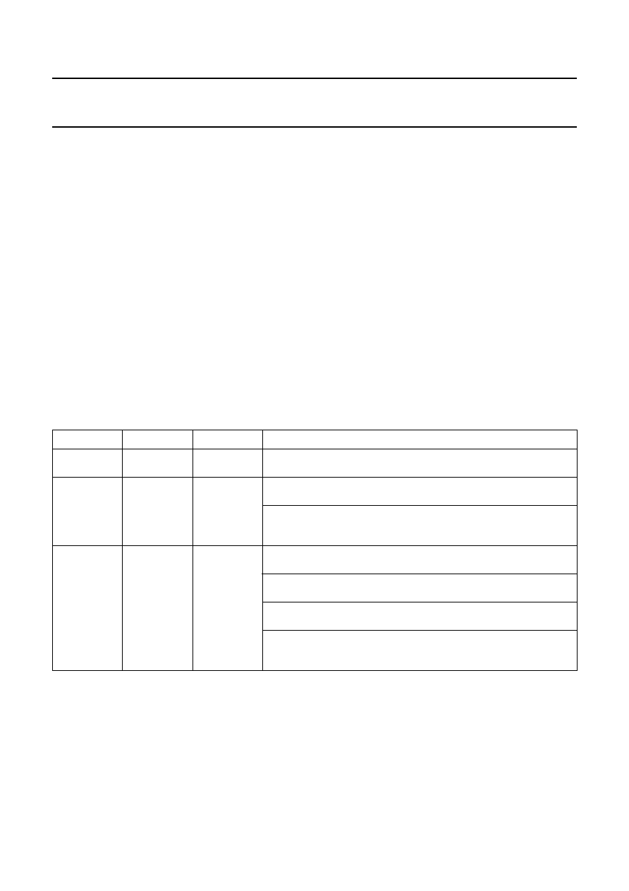
Table 2
Size, direction and purpose of the video FIFOs and the associated DMA controls
FIFO
SIZE
DIRECTION
PURPOSE
FIFO 1
128 Dwords
write to PCI
FIFO 1 buffers data from the HPS output and writes into PCI memory.
In planar mode FIFO 1 gets the Y data.
FIFO 2
128 Dwords
RW
Planar mode: FIFO 2 buffers U data provided by the HPS; the
associated DMA control 2 sends it into the PCI memory.
Clip mode: DMA control 2 reads clipping information (clip bit mask or
rectangular overlay data) from the PCI system memory and buffers it
in FIFO 2.
FIFO 3
128 Dwords
RW
Planar mode: FIFO 3 buffers V data provided by the HPS and writes
it into the PCI memory.
Chroma keying mode: FIFO 3 buffers chroma keying information
and writes it into PCI memory.
BRS mode: FIFO 3 buffers data provided by the BRS. DMA control 3
sends it into the PCI memory.
Read mode: DMA control 3 reads video data from the PCI system
memory (the same data up to four times to offer a simple upscaling
algorithm) and buffers it in FIFO 3.
相關(guān)PDF資料 |
PDF描述 |
|---|---|
| 935260698557 | SPECIALTY CONSUMER CIRCUIT, PQFP160 |
| 935260699551 | SPECIALTY CONSUMER CIRCUIT, PQFP208 |
| 935260699557 | SPECIALTY CONSUMER CIRCUIT, PQFP208 |
| 935243450551 | COLOR SIGNAL ENCODER, PQFP44 |
| 935243450557 | COLOR SIGNAL ENCODER, PQFP44 |
相關(guān)代理商/技術(shù)參數(shù) |
參數(shù)描述 |
|---|---|
| 935261069122 | 制造商:NXP Semiconductors 功能描述:IC SECURITY TRANSPONDER PLLMC |
| 935262025112 | 制造商:NXP Semiconductors 功能描述:SUB ONLY IC |
| 935262217118 | 制造商:NXP Semiconductors 功能描述:Real Time Clock Serial 8-Pin SO T/R |
| 935264217557 | 制造商:NXP Semiconductors 功能描述:SUB ONLY IC |
| 935267356112 | 制造商:NXP Semiconductors 功能描述:IC TEA1507PN |
發(fā)布緊急采購,3分鐘左右您將得到回復(fù)。