- 您現(xiàn)在的位置:買(mǎi)賣(mài)IC網(wǎng) > PDF目錄36334 > 935260017551 (NXP SEMICONDUCTORS) SPECIALTY CONSUMER CIRCUIT, PQFP64 PDF資料下載
參數(shù)資料
| 型號(hào): | 935260017551 |
| 廠商: | NXP SEMICONDUCTORS |
| 元件分類(lèi): | 消費(fèi)家電 |
| 英文描述: | SPECIALTY CONSUMER CIRCUIT, PQFP64 |
| 封裝: | PLASTIC, SOT-314, LQFP-64 |
| 文件頁(yè)數(shù): | 56/75頁(yè) |
| 文件大?。?/td> | 479K |
| 代理商: | 935260017551 |
第1頁(yè)第2頁(yè)第3頁(yè)第4頁(yè)第5頁(yè)第6頁(yè)第7頁(yè)第8頁(yè)第9頁(yè)第10頁(yè)第11頁(yè)第12頁(yè)第13頁(yè)第14頁(yè)第15頁(yè)第16頁(yè)第17頁(yè)第18頁(yè)第19頁(yè)第20頁(yè)第21頁(yè)第22頁(yè)第23頁(yè)第24頁(yè)第25頁(yè)第26頁(yè)第27頁(yè)第28頁(yè)第29頁(yè)第30頁(yè)第31頁(yè)第32頁(yè)第33頁(yè)第34頁(yè)第35頁(yè)第36頁(yè)第37頁(yè)第38頁(yè)第39頁(yè)第40頁(yè)第41頁(yè)第42頁(yè)第43頁(yè)第44頁(yè)第45頁(yè)第46頁(yè)第47頁(yè)第48頁(yè)第49頁(yè)第50頁(yè)第51頁(yè)第52頁(yè)第53頁(yè)第54頁(yè)第55頁(yè)當(dāng)前第56頁(yè)第57頁(yè)第58頁(yè)第59頁(yè)第60頁(yè)第61頁(yè)第62頁(yè)第63頁(yè)第64頁(yè)第65頁(yè)第66頁(yè)第67頁(yè)第68頁(yè)第69頁(yè)第70頁(yè)第71頁(yè)第72頁(yè)第73頁(yè)第74頁(yè)第75頁(yè)
1998 May 15
6
Philips Semiconductors
Product specication
Enhanced Video Input Processor (EVIP)
SAA7111A
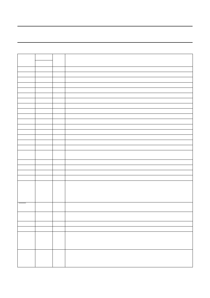
7
PINNING
SYMBOL
PIN
I/O/P
DESCRIPTION
(L)QFP64
n.c.
1
Do not connect.
TDO
2
O
Test data output for boundary scan test; note 1.
TDI
3
I
Test data input for boundary scan test; note 1.
TMS
4
I
Test mode select input for boundary scan test or scan test; note 1.
VSSA2
5
P
Ground for analog supply voltage channel 2.
AI22
6
I
Analog input 22.
VDDA2
7
P
Positive supply voltage for analog channel 2 (+3.3 V).
AI21
8
I
Analog input 21.
VSSA1
9
P
Ground for analog supply voltage channel 1.
AI12
10
I
Analog input 12.
VDDA1
11
P
Positive supply voltage for analog channel 1 (+3.3 V).
AI11
12
I
Analog input 11.
VSSS
13
P
Substrate ground connection.
AOUT
14
O
Analog test output; for testing the analog input channels.
VDDA0
15
P
Positive supply voltage for internal Clock Generator Circuit (CGC) (+3.3 V).
VSSA0
16
P
Ground for internal CGC.
VREF
17
O
Vertical reference output signal (I2C-bit COMPO = 0) or inverse composite blanking
signal (I2C-bit COMPO = 1) (enabled via I2C-bus bit OEHV).
VDDD5
18
P
Digital supply voltage 5 (+3.3 V).
VSSD5
19
P
Ground for digital supply voltage 5.
LLC
20
O
Line-locked system clock output (27 MHz).
LLC2
21
O
Line-locked clock 1
2 output (13.5 MHz).
CREF
22
O
Clock reference output: this is a clock qualier signal distributed by the internal CGC
for a data rate of LLC2. Using CREF all interfaces on the VPO bus are able to
generate a bus timing with identical phase. If CCIR 656 format is selected
(OFTS0 = 1 and OFTS1 = 1) an inverse composite blanking signal (pixel qualier) is
provided on this pin.
RES
23
O
Reset output (active LOW); sets the device into a dened state. All data outputs are
in high impedance state. The I2C-bus is reset (waiting for start condition).
CE
24
I
Chip enable; connection to ground forces a reset, up from version 3 power save
function additionally available.
VDDD4
25
P
Digital supply voltage input 4 (+3.3 V).
VSSD4
26
P
Ground for digital supply voltage input 4.
HS
27
O
Horizontal sync output signal (programmable); the positions of the positive and
negative slopes are programmable in 8 LLC increments over a complete line
(equals 64
s) via I2C-bus bytes HSB and HSS. Fine position adjustment in 2 LLC
increments can be performed via I2C-bus bits HDEL1 and HDEL0.
RTS1
28
O
Two functions output; controlled by I2C-bus bit RTSE1.
RTSE1 = 0: PAL line identier (LOW = PAL line); indicates the inverted and
non-inverted R
Y component for PAL signals. RTSE1 = 1: H-PLL locked indicator;
a high state indicates that the internal horizontal PLL has locked.
相關(guān)PDF資料 |
PDF描述 |
|---|---|
| 935260017557 | SPECIALTY CONSUMER CIRCUIT, PQFP64 |
| 935260018551 | SPECIALTY CONSUMER CIRCUIT, PQFP64 |
| 935260018557 | SPECIALTY CONSUMER CIRCUIT, PQFP64 |
| 935263652557 | SPECIALTY CONSUMER CIRCUIT, PQFP64 |
| 935233400112 | SPECIALTY CONSUMER CIRCUIT, PDIP24 |
相關(guān)代理商/技術(shù)參數(shù) |
參數(shù)描述 |
|---|---|
| 935260093112 | 制造商:NXP Semiconductors 功能描述:IC AVIC ADV BASESTATION 14SOIC |
| 935261069122 | 制造商:NXP Semiconductors 功能描述:IC SECURITY TRANSPONDER PLLMC |
| 935262025112 | 制造商:NXP Semiconductors 功能描述:SUB ONLY IC |
| 935262217118 | 制造商:NXP Semiconductors 功能描述:Real Time Clock Serial 8-Pin SO T/R |
| 935264217557 | 制造商:NXP Semiconductors 功能描述:SUB ONLY IC |
發(fā)布緊急采購(gòu),3分鐘左右您將得到回復(fù)。