- 您現(xiàn)在的位置:買賣IC網(wǎng) > PDF目錄24798 > 935250080118 (NXP SEMICONDUCTORS) LVC/LCX/Z SERIES, QUAD 2-INPUT OR GATE, PDSO14 PDF資料下載
參數(shù)資料
| 型號: | 935250080118 |
| 廠商: | NXP SEMICONDUCTORS |
| 元件分類: | 門電路 |
| 英文描述: | LVC/LCX/Z SERIES, QUAD 2-INPUT OR GATE, PDSO14 |
| 封裝: | 4.40 MM, PLASTIC, SOT-402-1, TSSOP-14 |
| 文件頁數(shù): | 3/10頁 |
| 文件大小: | 85K |
| 代理商: | 935250080118 |
Philips Semiconductors
Product specification
74LVC32A
Quad 2-input OR gate
2
1997 Jun 30
853-1995 18166
FEATURES
Wide supply voltage range of 1.2 V to 3.6 V
In accordance with JEDEC standard no. 8-1A.
Inputs accept voltages up to 5.5 V
CMOS low power consumption
Direct interface with TTL levels
DESCRIPTION
The 74LVC32A is a high-performance, low-power, low-voltage
Si-gate CMOS device and superior to most advanced CMOS
compatible TTL families.
Inputs can be driven from either 3.3V or 5V devices. This feature
allows the use of these devices as translators in a mixed 3.3V/5V
environment.
The 74LVC32A provides the 2-input OR function.
QUICK REFERENCE DATA
GND = 0 V; Tamb = 25°C; tr = tf ≤ 2.5 ns
SYMBOL
PARAMETER
CONDITIONS
TYPICAL
UNIT
tPHL/tPLH
Propagation delay
nA, nB to nY
CL = 50 pF;
VCC = 3.3 V
2.6
ns
CI
Input capacitance
5.0
pF
CPD
Power dissipation capacitance per gate
Notes 1 and 2
28
pF
NOTES:
1. CPD is used to determine the dynamic power dissipation (PD in W)
PD = CPD × VCC2 × fi ) (CL × VCC2 × fo) where:
fi = input frequency in MHz; CL = output load capacity in pF;
fo = output frequency in MHz; VCC = supply voltage in V;
(CL × VCC2 × fo) = sum of the outputs.
2. The condition is VI = GND to VCC.
ORDERING INFORMATION
PACKAGES
TEMPERATURE RANGE
OUTSIDE NORTH AMERICA
NORTH AMERICA
DWG NUMBER
14-Pin Plastic SO
–40
°C to +85°C
74LVC32A D
SOT108-1
14-Pin Plastic SSOP Type II
–40
°C to +85°C
74LVC32A DB
SOT337-1
14-Pin Plastic TSSOP Type I
–40
°C to +85°C
74LVC32A PW
74LVC32APW DH
SOT402-1
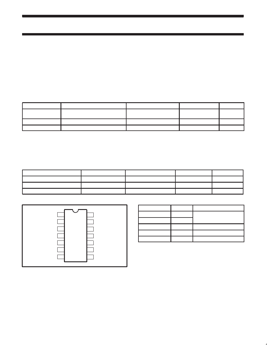
PIN CONFIGURATION
1
2
3
4
5
6
7
1A
1B
1Y
2A
2B
2Y
GND
V
CC
4B
4A
4Y
3B
3A
3Y
14
13
12
11
10
9
8
SV00450
PIN DESCRIPTION
PIN NUMBER
SYMBOL
NAME AND FUNCTION
1, 4, 9, 12
1A – 4A
Data inputs
2, 5, 10, 13
1B – 4B
Data inputs
3, 6, 8, 11
1Y – 4Y
Data outputs
7
GND
Ground (0 V)
14
VCC
Positive supply voltage
相關(guān)PDF資料 |
PDF描述 |
|---|---|
| 935250070112 | LVC/LCX/Z SERIES, QUAD 2-INPUT OR GATE, PDSO14 |
| 07-PX-1203 | AUTOMOTIVE 12VDC |
| 07-PX-2403 | AUTOMOTIVE 24VDC |
| 07-PXC-1203 | AUTOMOTIVE RELAIS 12VDC |
| 07-PXC-2403 | AUTOMOTIVE 24VDC |
相關(guān)代理商/技術(shù)參數(shù) |
參數(shù)描述 |
|---|---|
| 9-3525-012 | 制造商:KEYSTONE 功能描述:MODIFIED 3525,VERSION E |
| 935252-5 | 制造商:C-H 功能描述:935252-5 |
| 935257650112 | 制造商:NXP Semiconductors 功能描述:SUB ONLY ICSUBS TO 935257650112 |
| 935260093112 | 制造商:NXP Semiconductors 功能描述:IC AVIC ADV BASESTATION 14SOIC |
| 935261069122 | 制造商:NXP Semiconductors 功能描述:IC SECURITY TRANSPONDER PLLMC |
發(fā)布緊急采購,3分鐘左右您將得到回復(fù)。