- 您現(xiàn)在的位置:買賣IC網(wǎng) > PDF目錄36330 > 935089530518 (NXP SEMICONDUCTORS) SPECIALTY CONSUMER CIRCUIT, PQFP64 PDF資料下載
參數(shù)資料
| 型號(hào): | 935089530518 |
| 廠商: | NXP SEMICONDUCTORS |
| 元件分類: | 消費(fèi)家電 |
| 英文描述: | SPECIALTY CONSUMER CIRCUIT, PQFP64 |
| 封裝: | 14 X 20 MM, 2.80 MM HEIGHT, PLASTIC, SOT-319-2, QFP-64 |
| 文件頁數(shù): | 15/47頁 |
| 文件大小: | 250K |
| 代理商: | 935089530518 |
第1頁第2頁第3頁第4頁第5頁第6頁第7頁第8頁第9頁第10頁第11頁第12頁第13頁第14頁當(dāng)前第15頁第16頁第17頁第18頁第19頁第20頁第21頁第22頁第23頁第24頁第25頁第26頁第27頁第28頁第29頁第30頁第31頁第32頁第33頁第34頁第35頁第36頁第37頁第38頁第39頁第40頁第41頁第42頁第43頁第44頁第45頁第46頁第47頁
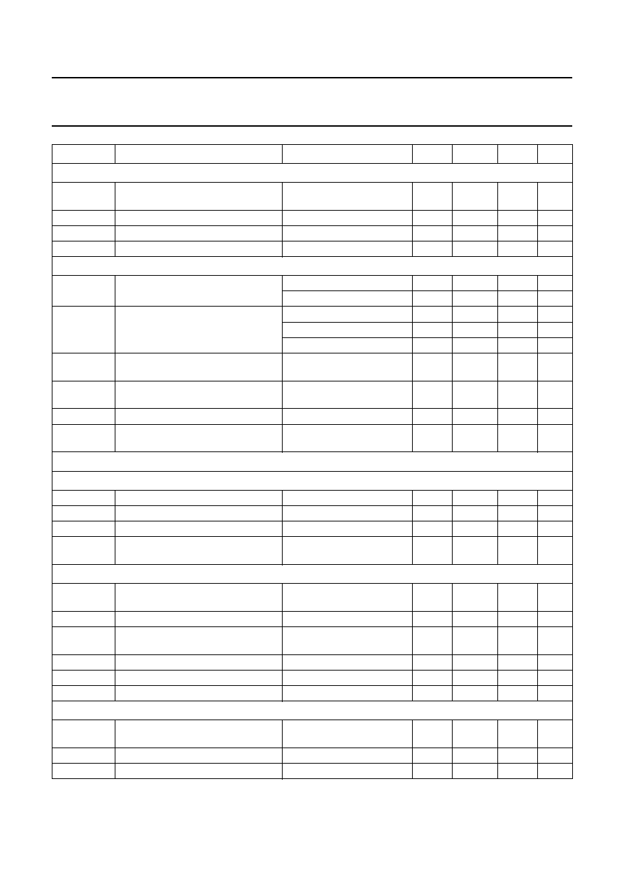
1996 Jan 26
22
Philips Semiconductors
Objective specication
I2C-bus controlled PAL/NTSC TV processors
TDA8376; TDA8376A
FLYBACK PULSE INPUT (PIN 41)
VHSW
switching voltage level for horizontal
blanking
0.4
V
V2(SW)
switching level for phase-2 loop
4.0
V
V41(max)
maximum input voltage
note 7
8.0
V
Zi
input impedance
note 7
10
M
SANDCASTLE PULSE OUTPUT (PIN 39)
V39
output voltage
during burst key
4.8
5.3
5.8
V
during blanking
1.8
2.0
2.2
V
tW
pulse width
burst key pulse
3.3
3.5
3.7
s
vertical blanking (50 Hz)
25
lines
vertical blanking (60 Hz)
21
lines
Vclamp
clamping voltage level for vertical
guard detection
2.7
V
I39(min)
minimum input current to activate
guard detection
0.5
mA
I39(max)
maximum allowable input current
2.5
mA
td
delay of start of burst key to start of
sync
5.4
s
Vertical synchronization and geometry correction
VERTICAL OSCILLATOR; note 15
ffr
free running frequency
50/60
Hz
flock
locking frequency range
45
64.5
Hz
divider value not locked
625/525
lines
LR
locking range
488
722
lines/
frame
VERTICAL RAMP GENERATOR (PIN 50)
V50(p-p)
sawtooth voltage amplitude
(peak-to-peak value)
VS = 1FH;
C = 100 nF; R = 39 k
3.5
V
Idis
discharge current
1
mA
Icharge
charge current set by external
resistor
note 16
19
A
VS
vertical slope control range
63 steps
20
+20
%
I
50
charge current increase
f = 60 Hz
20
%
V50L
LOW level voltage of ramp
2.07
V
VERTICAL DRIVE OUTPUTS (PINS 47 AND 48)
Idiff(p-p)
differential output current
(peak-to-peak value)
VA = 1FH
0.95
mA
ICM
common mode output current
400
A
Vo
output voltage
0
4.0
V
SYMBOL
PARAMETER
CONDITIONS
MIN.
TYP.
MAX.
UNIT
相關(guān)PDF資料 |
PDF描述 |
|---|---|
| 935071060157 | SPECIALTY CONSUMER CIRCUIT, PQFP80 |
| 935077580157 | SPECIALTY CONSUMER CIRCUIT, PQFP80 |
| 935206750518 | SPECIALTY CONSUMER CIRCUIT, PQFP80 |
| 935206750557 | SPECIALTY CONSUMER CIRCUIT, PQFP80 |
| 935075380112 | SPECIALTY CONSUMER CIRCUIT, PDSO28 |
相關(guān)代理商/技術(shù)參數(shù) |
參數(shù)描述 |
|---|---|
| 9350DC-200-0GZZZA | 制造商:Siemens 功能描述: |
| 9350DC-200-0ZZZTA | 制造商:Siemens 功能描述: |
| 9350DC-200-0ZZZZA | 制造商:Siemens 功能描述: |
| 9350-DISPLAY | 制造商:Siemens 功能描述: |
| 9350SC-100-0GZZZA | 制造商:Siemens 功能描述: |
發(fā)布緊急采購,3分鐘左右您將得到回復(fù)。