- 您現(xiàn)在的位置:買賣IC網(wǎng) > PDF目錄24768 > 935037570602 (NXP SEMICONDUCTORS) F/FAST SERIES, DUAL NEGATIVE EDGE TRIGGERED J-K FLIP-FLOP, COMPLEMENTARY OUTPUT, PDIP14 PDF資料下載
參數(shù)資料
| 型號: | 935037570602 |
| 廠商: | NXP SEMICONDUCTORS |
| 元件分類: | 鎖存器 |
| 英文描述: | F/FAST SERIES, DUAL NEGATIVE EDGE TRIGGERED J-K FLIP-FLOP, COMPLEMENTARY OUTPUT, PDIP14 |
| 封裝: | 0.300 INCH, PLASTIC, MO-001AA, SOT-27-1, DIP-14 |
| 文件頁數(shù): | 5/10頁 |
| 文件大小: | 91K |
| 代理商: | 935037570602 |
Philips Semiconductors
Product specification
74F113
Dual J-K negative edge-triggered flip-flops
without reset
1996 Mar 14
4
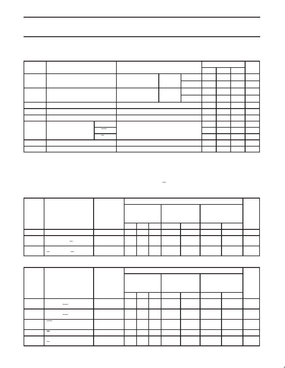
DC ELECTRICAL CHARACTERISTICS
(Over recommended operating free-air temperature range unless otherwise noted.)
SYMBOL
PARAMETER
TEST CONDITIONS1
LIMITS
UNIT
SYMBOL
PARAMETER
TEST CONDITIONS1
MIN
TYP2
MAX
UNIT
VO
High level output voltage
VCC = MIN, VIL = MAX,
IO = MAX
±10%V
CC
2.5
V
VOH
High-level output voltage
VCC
MIN, VIL
MAX,
VIH = MIN
IOH = MAX
±5%V
CC
2.7
3.4
V
VO
Low level output voltage
VCC = MIN, VIL = MAX,
IO = MAX
±10%V
CC
0.30
0.50
V
VOL
Low-level output voltage
VCC
MIN, VIL
MAX,
VIH = MIN
IOL = MAX
±5%V
CC
0.30
0.50
V
VIK
Input clamp voltage
VCC = MIN, II = IIK
–0.73
–1.2
V
II
Input current at maximum input voltage
VCC = MAX, VI = 7.0V
100
A
IIH
High-level input current
VCC = MAX, VI = 2.7V
20
A
Jn, Kn
–0.6
mA
IIL
Low-level input current
CPn
VCC = MAX, VI = 0.5V
–2.4
mA
SDn
–3.0
mA
IOS
Short-circuit output current3
VCC = MAX
-60
–150
mA
ICC
Supply current4 (total)
VCC = MAX
15
21
mA
NOTES:
1. For conditions shown as MIN or MAX, use the appropriate value specified under recommended operating conditions for the applicable type.
2. All typical values are at VCC = 5V, Tamb = 25°C.
3. Not more than one output should be shorted at a time. For testing IOS, the use of high-speed test apparatus and/or sample-and-hold
techniques are preferable in order to minimize internal heating and more accurately reflect operational values. Otherwise, prolonged shorting
of a high output may raise the chip temperature well above normal and thereby cause invalid readings in other parameter tests. In any
sequence of parameter tests, IOS tests should be performed last.
4. Measure ICC with the clock input grounded and all outputs open, then with Q and Q outputs high in turn.
AC ELECTRICAL CHARACTERISTICS
LIMITS
SYMBOL
PARAMETER
TEST
CONDITION
VCC = +5.0V
Tamb = +25°C
CL = 50pF
RL = 500
VCC = +5.0V ± 10%
Tamb = 0°C to +70°C
CL = 50pF
RL = 500
VCC = +5.0V ± 10%
Tamb = –40°C to +85°C
CL = 50pF
RL = 500
UNIT
MIN
TYP
MAX
MIN
MAX
MIN
MAX
fmax
Maximum clock frequency
Waveform 1
85
100
80
ns
tPLH
tPHL
Propagation delay
CPn to Qn or Qn
Waveform 1
2.0
4.0
6.0
2.0
7.0
2.0
7.5
7.0
ns
tPLH
tPHL
Propagation delay
SDn, to Qn or Qn
Waveform 2
2.0
4.5
6.5
2.0
7.5
2.0
8.0
7.5
ns
AC SETUP REQUIREMENTS
LIMITS
SYMBOL
PARAMETER
TEST
CONDITION
VCC = +5.0V
Tamb = +25°C
CL = 50pF
RL = 500
VCC = +5.0V ± 10%
Tamb = 0°C to +70°C
CL = 50pF
RL = 500
VCC = +5.0V ± 10%
Tamb = –40°C to +85°C
CL = 50pF
RL = 500
UNIT
MIN
TYP
MAX
MIN
MAX
MIN
MAX
tsu (H)
tsu(L)
Setup time, high or low
Jn, Kn to CPn
Waveform 1
4.0
3.5
5.0
4.0
5.0
4.5
ns
th (H)
th (L)
Hold time, high or low
Jn, Kn to CPn
Waveform 1
0.0
ns
tw (H)
tw (L)
CP pulse width,
high or low
Waveform 1
4.5
5.0
ns
tw (L)
SDn pulse width, low
Waveform 2
4.5
5.0
ns
trec
Recovery time
SDn to CPn
Waveform 2
4.5
5.0
ns
相關(guān)PDF資料 |
PDF描述 |
|---|---|
| 933861310623 | F/FAST SERIES, DUAL NEGATIVE EDGE TRIGGERED J-K FLIP-FLOP, COMPLEMENTARY OUTPUT, PDSO14 |
| 935037700602 | F/FAST SERIES, HEX 2-INPUT AND GATE, PDSO20 |
| 935037600623 | F/FAST SERIES, HEX 2-INPUT AND GATE, PDSO20 |
| 935037600602 | F/FAST SERIES, HEX 2-INPUT AND GATE, PDSO20 |
| 935037700623 | F/FAST SERIES, HEX 2-INPUT AND GATE, PDSO20 |
相關(guān)代理商/技術(shù)參數(shù) |
參數(shù)描述 |
|---|---|
| 9350-3R1 | 制造商:Johanson Manufacturing 功能描述:VARIABLE CAPACITOR |
| 935040870112 | 制造商:NXP Semiconductors 功能描述:IC MIXER FM IF SYSTEM LP 20-SSOP |
| 9350-4R1 | 制造商:Johanson Manufacturing 功能描述:VARIABLE CAPACITOR 制造商:Johanson 功能描述:VARIABLE CAPACITOR |
| 9350524523211N | 制造商:ESSEX 功能描述:ESSEX 32V/DC |
| 9350569 | 制造商:WIKA INSTRUMENTS 功能描述:1/8,1/4 GAUGE |
發(fā)布緊急采購,3分鐘左右您將得到回復(fù)。