- 您現(xiàn)在的位置:買賣IC網(wǎng) > PDF目錄24697 > 934055221118 (NXP SEMICONDUCTORS) 69 A, 25 V, 0.014 ohm, N-CHANNEL, Si, POWER, MOSFET PDF資料下載
參數(shù)資料
| 型號(hào): | 934055221118 |
| 廠商: | NXP SEMICONDUCTORS |
| 元件分類: | JFETs |
| 英文描述: | 69 A, 25 V, 0.014 ohm, N-CHANNEL, Si, POWER, MOSFET |
| 封裝: | PLASTIC, DPAK-3 |
| 文件頁(yè)數(shù): | 1/14頁(yè) |
| 文件大小: | 145K |
| 代理商: | 934055221118 |
當(dāng)前第1頁(yè)第2頁(yè)第3頁(yè)第4頁(yè)第5頁(yè)第6頁(yè)第7頁(yè)第8頁(yè)第9頁(yè)第10頁(yè)第11頁(yè)第12頁(yè)第13頁(yè)第14頁(yè)
Philips Semiconductors
Product specification
N-channel TrenchMOS
transistor
PHP69N03LT, PHB69N03LT
Logic level FET
PHD69N03LT
FEATURES
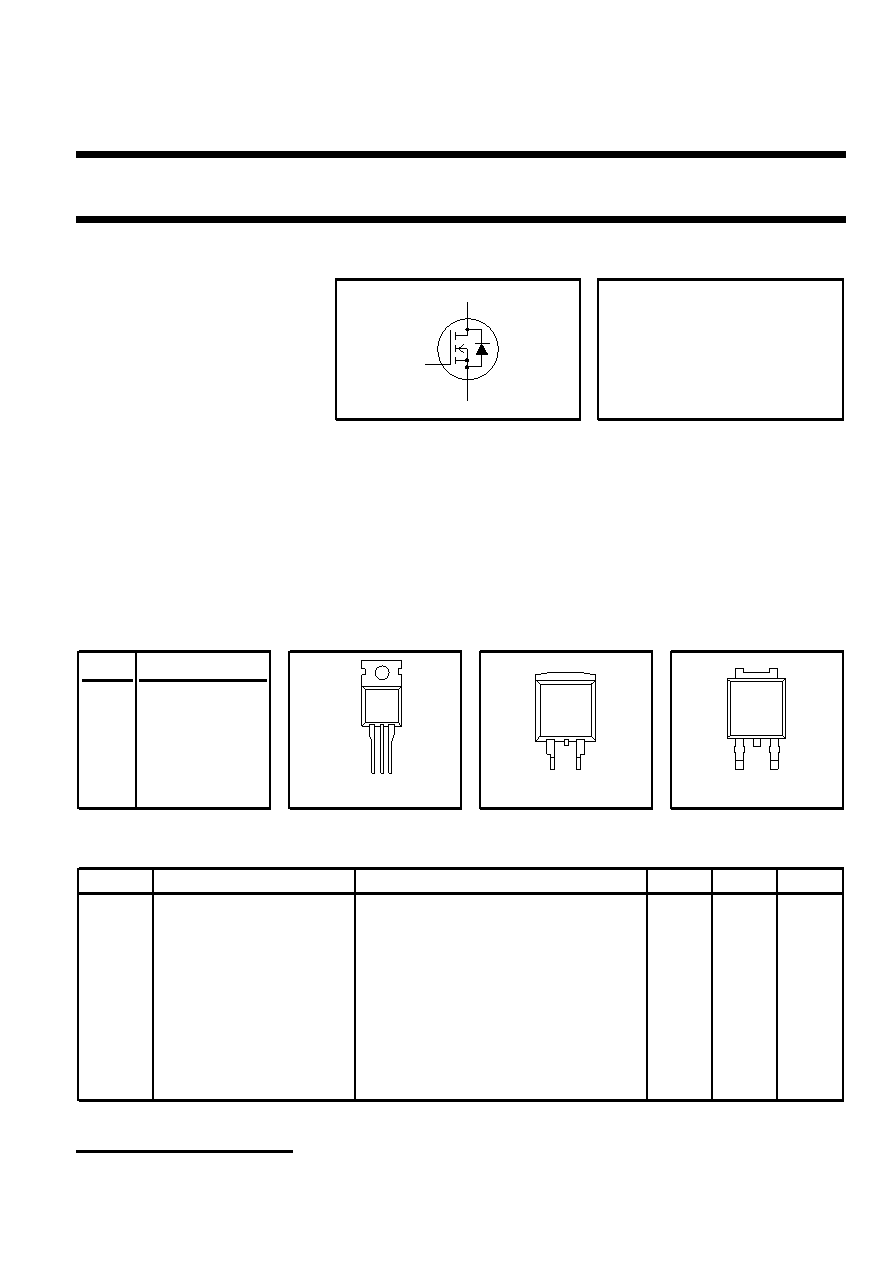
SYMBOL
QUICK REFERENCE DATA
’Trench’ technology
V
DSS = 25 V
Very low on-state resistance
Fast switching
I
D = 69 A
Low thermal resistance
Logic level compatible
R
DS(ON) ≤ 12 m (VGS = 10 V)
R
DS(ON) ≤ 14 m (VGS = 5 V)
GENERAL DESCRIPTION
N-channel enhancement mode logic level field-effect power transistor in a plastic envelope using ’trench’ technology.
Applications:-
High frequency computer motherboard d.c. to d.c. converters
High current switching
The PHP69N03LT is supplied in the SOT78 (TO220AB) conventional leaded package.
The PHB69N03LT is supplied in the SOT404 (D
2PAK) surface mounting package.
The PHD69N03LT is supplied in the SOT428 (DPAK)surface mounting package.
PINNING
SOT78 (TO220AB)
SOT404 (D
2PAK)
SOT428 (DPAK)
PIN
DESCRIPTION
1
gate
2
drain
1
3
source
tab
drain
LIMITING VALUES
Limiting values in accordance with the Absolute Maximum System (IEC 134)
SYMBOL PARAMETER
CONDITIONS
MIN.
MAX.
UNIT
V
DSS
Drain-source voltage
T
j = 25 C to 175C
-
25
V
DGR
Drain-gate voltage
T
j = 25 C to 175C; RGS = 20 k
-25
V
GS
Gate-source voltage (DC)
-
± 15
V
GSM
Gate-source voltage (pulse
T
j ≤ 150C
-
± 20
V
peak value)
I
D
Drain current (DC)
T
mb =
25 C
-
69
A
T
mb = 100 C
-
48
A
I
DM
Drain current (pulse peak
T
mb = 25 C
-
240
A
value)
P
tot
Total power dissipation
T
mb = 25 C
-
125
W
T
j, Tstg
Operating junction and
- 55
175
C
storage temperature
d
g
s
12 3
tab
13
tab
2
1
2
3
tab
1 It is not possible to make connection to pin:2 of the SOT404 or SOT428 packages.
October 1999
1
Rev 1.600
發(fā)布緊急采購(gòu),3分鐘左右您將得到回復(fù)。