- 您現(xiàn)在的位置:買賣IC網(wǎng) > PDF目錄375094 > 7C421-30 (Cypress Semiconductor Corp.) 256/512/1K/2K/4K x 9 Asynchronous FIFO PDF資料下載
參數(shù)資料
| 型號: | 7C421-30 |
| 廠商: | Cypress Semiconductor Corp. |
| 英文描述: | 256/512/1K/2K/4K x 9 Asynchronous FIFO |
| 中文描述: | 256/512/1K/2K/4K × 9異步FIFO |
| 文件頁數(shù): | 5/22頁 |
| 文件大小: | 522K |
| 代理商: | 7C421-30 |
CY7C419/21/25/29/33
Document #: 38-06001 Rev. *A
Page 5 of 22
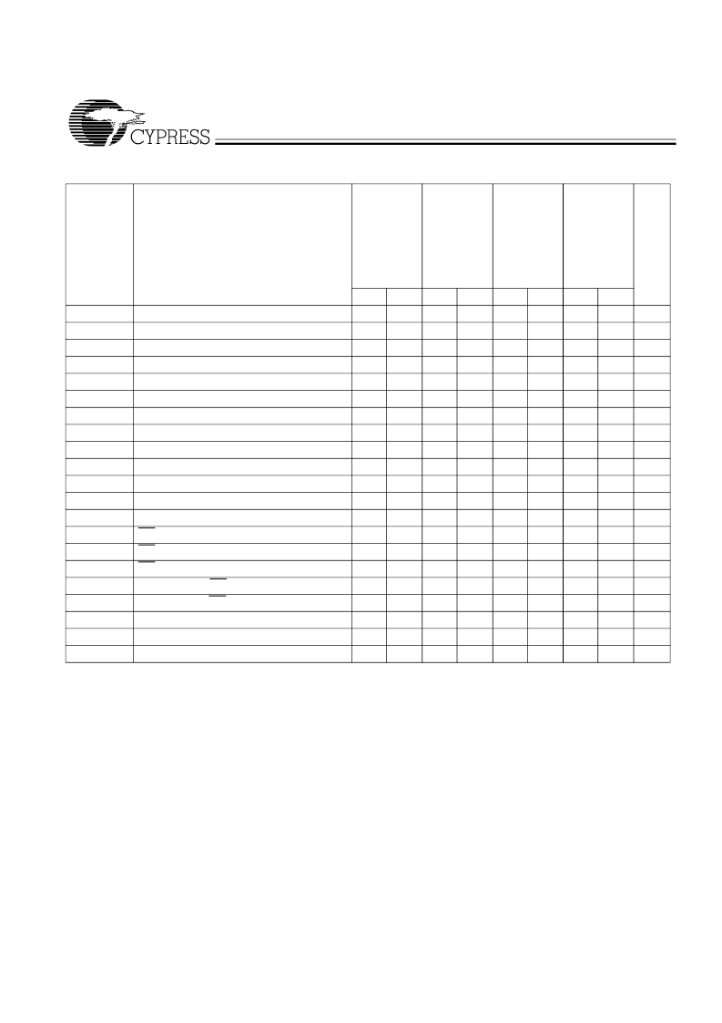
Switching Characteristics
Over the Operating Range
[7, 8]
7C419
–
10
7C421
–
10
7C425
–
10
7C429
–
10
7C433
–
10
Min.
20
7C419
–
15
7C421
–
15
7C425
–
15
7C429
–
15
7C433
–
15
Min.
25
7C420
–
20
7C421
–
20
7C424
–
20
7C425
–
20
7C428
–
20
7C429
–
20
7C433
–
20
Min.
30
7C420
–
25
7C421
–
25
7C424
–
25
7C425
–
25
7C429
–
25
7C432
–
25
7C433
–
25
Min.
35
Parameter
t
RC
t
A
t
RR
t
PR
t
LZR[6,9]
t
DVR[9,10]
t
HZR[6,9,10]
t
WC
t
PW
t
HWZ[6,9]
t
WR
t
SD
t
HD
t
MRSC
t
PMR
t
RMR
t
RPW
t
WPW
t
RTC
t
PRT
t
RTR
Notes:
7.
Test conditions assume signal transition time of 3 ns or less, timing reference levels of 1.5V and output loading of the specified I
OL
/I
OH
and 30 pF load
capacitance, as in part (a) of AC Test Load and Waveforms, unless otherwise specified.
8.
See the last page of this specification for Group A subgroup testing information.
9.
t
HZR
transition is measured at +200 mV from V
OL
and
–
200 mV from V
OH
. t
DVR
transition is measured at the 1.5V level. t
HWZ
and t
LZR
transition is measured
at
±
100 mV from the steady state.
10. t
HZR
and t
DVR
use capacitance loading as in part (b) of AC Test Load and Waveforms.
Description
Max.
Max.
Max.
Max.
Unit
ns
ns
ns
ns
ns
ns
ns
ns
ns
ns
ns
ns
ns
ns
ns
ns
ns
ns
ns
ns
ns
Read Cycle Time
Access Time
Read Recovery Time
Read Pulse Width
Read LOW to Low Z
Data Valid After Read HIGH
Read HIGH to High Z
Write Cycle Time
Write Pulse Width
Write HIGH to Low Z
Write Recovery Time
Data Set-Up Time
Data Hold Time
MR Cycle Time
MR Pulse Width
MR Recovery Time
Read HIGH to MR HIGH
Write HIGH to MR HIGH
Retransmit Cycle Time
Retransmit Pulse Width
Retransmit Recovery Time
10
15
20
25
10
10
3
5
10
15
3
5
10
20
3
5
10
25
3
5
15
15
15
18
20
10
5
10
6
0
20
10
10
10
10
20
10
10
25
15
5
10
8
0
25
15
10
15
15
25
15
10
30
20
5
10
12
0
30
20
10
20
20
30
20
10
35
25
5
10
15
0
35
25
10
25
25
35
25
10
相關PDF資料 |
PDF描述 |
|---|---|
| 7C421-40 | 256/512/1K/2K/4K x 9 Asynchronous FIFO |
| 7C421-65 | 256/512/1K/2K/4K x 9 Asynchronous FIFO |
| 7C425-10 | 256/512/1K/2K/4K x 9 Asynchronous FIFO |
| 7C425-15 | 256/512/1K/2K/4K x 9 Asynchronous FIFO |
| 7C425-20 | 256/512/1K/2K/4K x 9 Asynchronous FIFO |
相關代理商/技術參數(shù) |
參數(shù)描述 |
|---|---|
| 7C421-30DMB | 制造商: 功能描述: 制造商:undefined 功能描述: |
| 7C421-40 | 制造商:CYPRESS 制造商全稱:Cypress Semiconductor 功能描述:256/512/1K/2K/4K x 9 Asynchronous FIFO |
| 7C4215AT | 制造商:Cypress Semiconductor 功能描述: |
| 7C421-65 | 制造商:CYPRESS 制造商全稱:Cypress Semiconductor 功能描述:256/512/1K/2K/4K x 9 Asynchronous FIFO |
| 7C421DT | 制造商:Cypress Semiconductor 功能描述: |
發(fā)布緊急采購,3分鐘左右您將得到回復。