- 您現(xiàn)在的位置:買賣IC網(wǎng) > PDF目錄375093 > 7C199-10 (Cypress Semiconductor Corp.) 32K x 8 Static RAM PDF資料下載
參數(shù)資料
| 型號: | 7C199-10 |
| 廠商: | Cypress Semiconductor Corp. |
| 英文描述: | 32K x 8 Static RAM |
| 中文描述: | 32K的× 8靜態(tài)RAM |
| 文件頁數(shù): | 4/13頁 |
| 文件大?。?/td> | 317K |
| 代理商: | 7C199-10 |
CY7C199
Document #: 38-05160 Rev. *A
Page 4 of 13
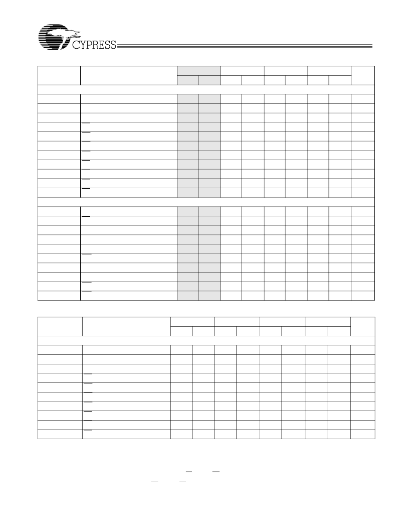
Switching Characteristics
Over the Operating Range (-8, -10, -12, -15)
[3, 7]
Parameter
Read Cycle
t
RC
t
AA
t
OHA
t
ACE
t
DOE
t
LZOE
t
HZOE
t
LZCE
t
HZCE
t
PU
t
PD
Write Cycle
[10, 11]
t
WC
t
SCE
t
AW
t
HA
t
SA
t
PWE
t
SD
t
HD
t
HZWE
t
LZWE
Description
7C199-8
Min.
7C199-10
Min.
7C199-12
Min.
7C199-15
Min.
Unit
Max.
Max.
Max.
Max.
Read Cycle Time
Address to Data Valid
Data Hold from Address Change
CE LOW to Data Valid
OE LOW to Data Valid
OE LOW to Low-Z
[8]
OE HIGH to High-Z
[8, 9]
CE LOW to Low-Z
[8]
CE HIGH to High-Z
[8,9]
CE LOW to Power-up
CE HIGH to Power-down
8
10
12
15
ns
ns
ns
ns
ns
ns
ns
ns
ns
ns
ns
8
10
12
15
3
3
3
3
8
10
5
12
5
15
7
4.5
0
0
0
0
5
5
5
7
3
3
3
3
4
5
5
7
0
0
0
0
8
10
12
15
Write Cycle Time
CE LOW to Write End
Address Set-up to Write End
Address Hold from Write End
Address Set-up to Write Start
WE Pulse Width
Data Set-up to Write End
Data Hold from Write End
WE LOW to High-Z
[9]
WE HIGH to Low-Z
[8]
8
7
7
0
0
7
5
0
10
7
7
0
0
7
5
0
12
9
9
0
0
8
8
0
15
10
10
0
0
9
9
0
ns
ns
ns
ns
ns
ns
ns
ns
ns
ns
5
6
7
7
3
3
3
3
Switching Characteristics
Over the Operating Range (-20, -25, -35, -45)
[3, 7]
Parameter
Read Cycle
t
RC
t
AA
t
OHA
t
ACE
t
DOE
t
LZOE
t
HZOE
t
LZCE
t
HZCE
t
PU
Shaded area contains advance information.
Notes:
7.
Test conditions assume signal transition time of 3 ns or less for -12 and -15 speeds and 5 ns or less for -20 and slower speeds, timing reference levels of 1.5V,
input pulse levels of 0 to 3.0V, and output loading of the specified I
OL
/I
OH
and 30-pF load capacitance.
8.
At any given temperature and voltage condition, t
is less than t
, t
is less than t
, and t
HZWE
is less than t
LZWE
for any given device.
9.
t
, t
, and t
are specified with C
= 5 pF as in part (b) of AC Test Loads. Transition is measured
±
10. The internal write time of the memory is defined by the overlap of CE LOW and WE LOW. Both signals must be LOW to initiate a write and either signal can terminate
a write by going HIGH. The data input set-up and hold timing should be referenced to the rising edge of the signal that terminates the write.
11.
The minimum write cycle time for write cycle #3 (WE controlled, OE LOW) is the sum of t
HZWE
and t
SD
.
Description
7C199-20
Min.
7C199-25
Min.
7C199-35
Min.
7C199-45
Min.
Unit
Max.
Max.
Max.
Max.
Read Cycle Time
Address to Data Valid
Data Hold from Address Change
CE LOW to Data Valid
OE LOW to Data Valid
OE LOW to Low-Z
[8]
OE HIGH to High-Z
[8, 9]
CE LOW to Low-Z
[8]
CE HIGH to High-Z
[8, 9]
CE LOW to Power-up
20
25
35
45
ns
ns
ns
ns
ns
ns
ns
ns
ns
ns
20
25
35
45
3
3
3
3
20
9
25
10
35
16
45
16
0
0
0
0
9
11
15
15
3
3
3
3
9
11
15
15
0
0
0
0
相關(guān)PDF資料 |
PDF描述 |
|---|---|
| 7C199-20 | 32K x 8 Static RAM |
| 7C374I-100 | UltraLogic 128-Macrocell Flash CPLD |
| 7C374I-125 | UltraLogic 128-Macrocell Flash CPLD |
| 7C374I-66 | UltraLogic 128-Macrocell Flash CPLD |
| 7C374I-83 | UltraLogic 128-Macrocell Flash CPLD |
相關(guān)代理商/技術(shù)參數(shù) |
參數(shù)描述 |
|---|---|
| 7C199-12 | 制造商:CYPRESS 制造商全稱:Cypress Semiconductor 功能描述:32K x 8 Static RAM |
| 7C199-15 | 制造商:CYPRESS 制造商全稱:Cypress Semiconductor 功能描述:32K x 8 Static RAM |
| 7C199-20 | 制造商:CYPRESS 制造商全稱:Cypress Semiconductor 功能描述:32K x 8 Static RAM |
| 7C199-25 | 制造商:CYPRESS 制造商全稱:Cypress Semiconductor 功能描述:32K x 8 Static RAM |
| 7C199-35 | 制造商:CYPRESS 制造商全稱:Cypress Semiconductor 功能描述:32K x 8 Static RAM |
發(fā)布緊急采購,3分鐘左右您將得到回復(fù)。