- 您現(xiàn)在的位置:買賣IC網(wǎng) > PDF目錄375093 > 7C192-25 (Cypress Semiconductor Corp.) 64K x 4 Static RAM with Separate I/O PDF資料下載
參數(shù)資料
| 型號: | 7C192-25 |
| 廠商: | Cypress Semiconductor Corp. |
| 英文描述: | 64K x 4 Static RAM with Separate I/O |
| 中文描述: | 64K的× 4靜態(tài)存儲器具有獨(dú)立的I / O |
| 文件頁數(shù): | 4/10頁 |
| 文件大小: | 172K |
| 代理商: | 7C192-25 |
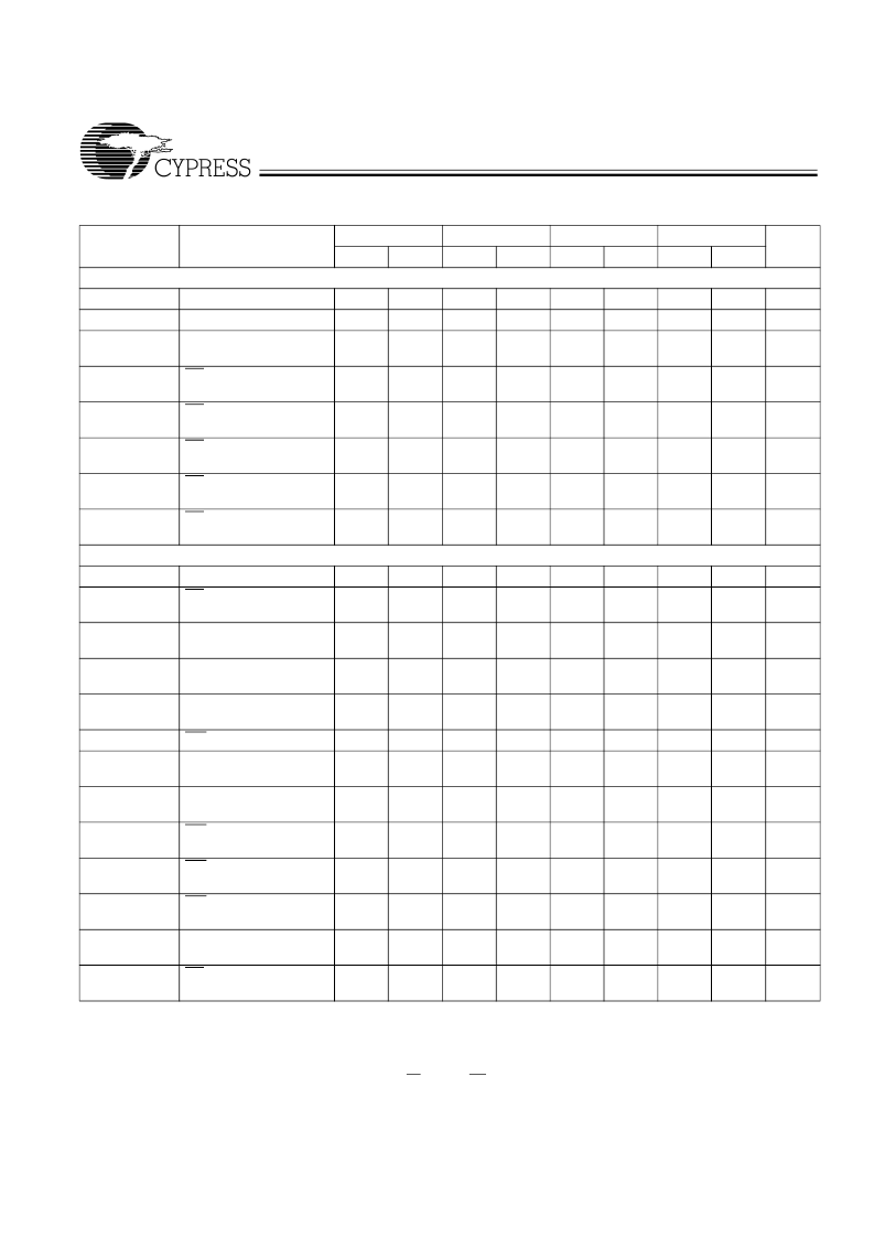
CY7C192
Document #: 38-05047 Rev. **
Page 4 of 10
Switching Characteristics
Over the Operating Range
[6]
7C192-12
Min.
7C192-15
Min.
7C192-20
Min.
7C192-25
Min.
Parameter
READ CYCLE
t
RC
t
AA
t
OHA
Description
Max.
Max.
Max.
Max.
Unit
Read Cycle Time
Address to Data Valid
Output Hold from
Address Change
CE LOW to
Data Valid
CE LOW to
Low Z
[7]
CE HIGH to
High Z
[7,8]
CE LOW to
Power-Up
CE HIGH to
Power-Down
12
15
20
25
ns
ns
ns
12
15
20
25
3
3
3
3
t
ACE
12
15
20
25
ns
t
LZCE
3
3
3
3
ns
t
HZCE
5
7
9
11
ns
t
PU
0
0
0
0
ns
t
PD
12
15
20
25
ns
WRITE CYCLE
[9]
t
WC
t
SCE
Write Cycle Time
CE LOW to
Write End
Address Set-Up to
Write End
Address Hold from
Write End
Address Set-Up to
Write Start
WE Pulse Width
Data Set-Up to
Write End
Data Hold from
Write End
WE HIGH to
Low Z (7C192)
[7]
WE LOW to
High Z (7C192)
[7,8]
WE LOW to Data Valid
(7C191)
Data Valid to
Output Valid (7C191)
CE LOW to Data Valid
(7C191)
12
9
15
10
20
15
25
18
ns
ns
t
AW
9
10
15
20
ns
t
HA
0
0
0
0
ns
t
SA
0
0
0
0
ns
t
PWE
t
SD
8
8
9
9
15
10
18
10
ns
ns
t
HD
0
0
0
0
ns
t
LZWE
3
3
3
3
ns
t
HZWE
7
7
10
11
ns
t
DWE
12
15
20
25
ns
t
ADV
12
15
20
20
ns
t
DCE
12
15
20
25
ns
Notes:
6.
Test conditions assume signal transition time of 3 ns or less for -12 and -15 speeds and 5 ns or less for -20 through -25 speeds, timing reference levels of
1.5V, input pulse levels of 0 to 3.0V, and output loading of the specified I
OL
/I
OH
and 30-pF load capacitance.
At any given temperature and voltage condition, t
HZCE
is less than t
LZCE
, t
HZWE
is less than t
LZWE
for any given device. These parameters are guaranteed by
design and not 100% tested.
t
and t
are specified with C
= 5 pF as in part (b) of AC Test Loads. Transition is measured
±
500 mV from steady-state voltage.
The internal write time of the memory is defined by the overlap of CE LOW and WE LOW. Both signals must be LOW to initiate a write and either signal can
terminate a write by going HIGH. The data input set-up and hold timing should be referenced to the rising edge of the signal that terminates the write.
7.
8.
9.
相關(guān)PDF資料 |
PDF描述 |
|---|---|
| 7C199-12 | 32K x 8 Static RAM |
| 7C199-15 | 32K x 8 Static RAM |
| 7C199-25 | 32K x 8 Static RAM |
| 7C199-35 | 32K x 8 Static RAM |
| 7C199-45 | 32K x 8 Static RAM |
相關(guān)代理商/技術(shù)參數(shù) |
參數(shù)描述 |
|---|---|
| 7C1925DT WAF | 制造商:Cypress Semiconductor 功能描述: |
| 7C192C | 制造商:Cypress Semiconductor 功能描述: |
| 7C192HT | 制造商:Cypress Semiconductor 功能描述: |
| 7C194C | 制造商:Cypress Semiconductor 功能描述: |
| 7C194D | 制造商:Cypress Semiconductor 功能描述: |
發(fā)布緊急采購,3分鐘左右您將得到回復(fù)。