- 您現(xiàn)在的位置:買賣IC網(wǎng) > PDF目錄375093 > 7C1351-40 (Cypress Semiconductor Corp.) 128Kx36 Flow-Through SRAM with NoBL TM Architecture PDF資料下載
參數(shù)資料
| 型號: | 7C1351-40 |
| 廠商: | Cypress Semiconductor Corp. |
| 英文描述: | 128Kx36 Flow-Through SRAM with NoBL TM Architecture |
| 中文描述: | 128K × 36至流通過與總線延遲TM架構(gòu)的SRAM |
| 文件頁數(shù): | 11/13頁 |
| 文件大小: | 195K |
| 代理商: | 7C1351-40 |
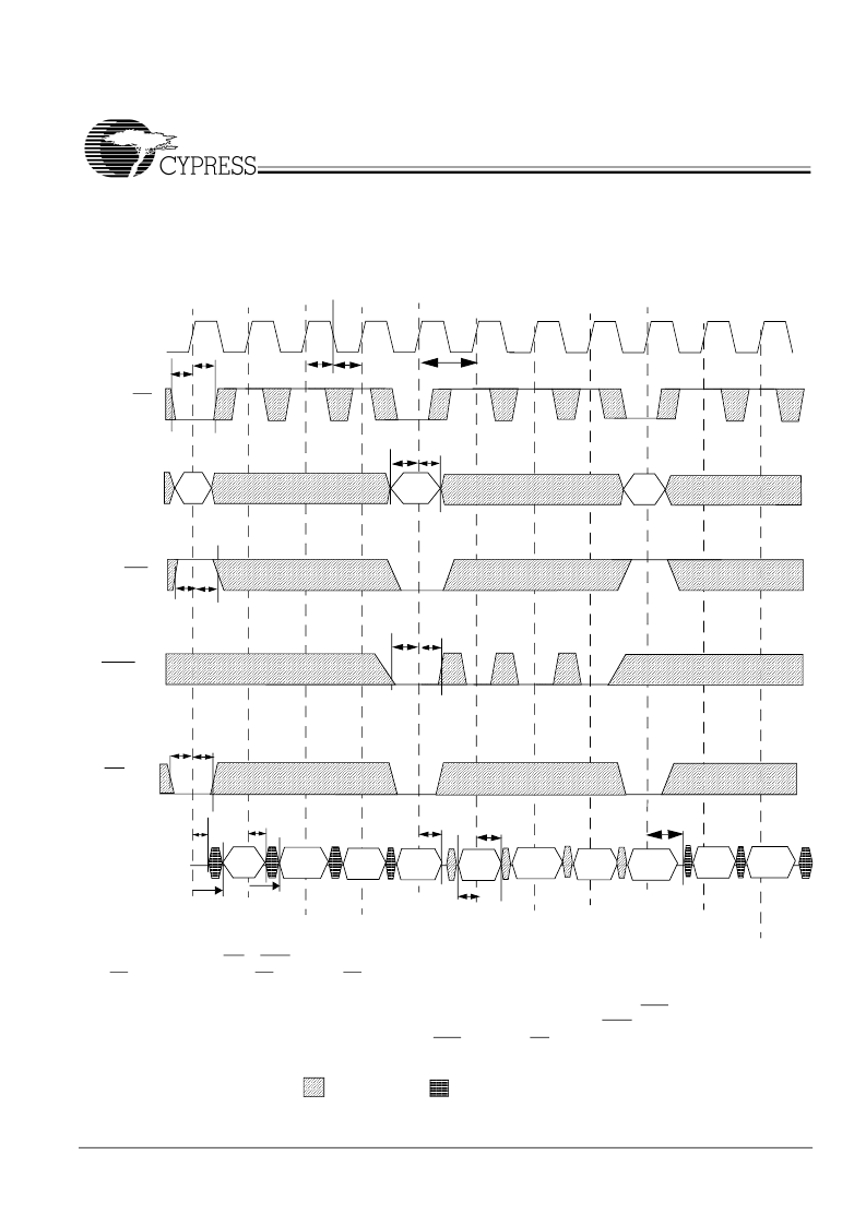
CY7C1351
11
Switching Waveforms
(continued)
ADV/LD
CLK
ADDRESS
CE
1a
Data-
In/Out
t
CYC
t
CH
t
CL
t
ALS
t
ALH
RA1
t
AH
t
AS
t
CES
t
CEH
t
CDV
Q1
Out
= DON
’
T CARE
= UNDEFINED
The combination of WE & BWS
[3:0]
defines a write cycle (see Write Cycle Description table).
CE is the combination of CE
1
, CE
2
, and CE
3
. All chip enables need to be active in order to select
the device. Any chip enable can deselect the device. RAx stands for Read Address X, WAx stands for
Write Address X, Dx stands for Data-in for location X, Qx stands for Data-out for location X. CEN held
LOW. During burst writes, byte writes can be conducted by asserting the appropriate BWS
[3:0]
input signals.
Burst order determined by the state of the MODE input. CEN held LOW. OE held LOW.
B
B
t
CLZ
t
DOH
Device
originally deselected
WA2
Q1+1
Out
Q1+2
Out
Q1+3
Out
RA3
t
CLZ
t
CHZ
D2+1
In
D2+2
In
D2+3
In
D2
In
t
CDV
Q3
Out
t
DS
t
DH
B
B
B
B
B
B
B
B
B
Burst Sequences
WS
[3:0]
t
WS
t
WH
WE
t
WS
t
WH
Out
Q3+1
相關(guān)PDF資料 |
PDF描述 |
|---|---|
| 7C1351-50 | 128Kx36 Flow-Through SRAM with NoBL TM Architecture |
| 7C1351-66 | 128Kx36 Flow-Through SRAM with NoBL TM Architecture |
| 7C1359A-100 | 256K x 18 Synchronous-Pipelined Cache Tag RAM |
| 7C1359A-133 | 256K x 18 Synchronous-Pipelined Cache Tag RAM |
| 7C1359A-150 | 256K x 18 Synchronous-Pipelined Cache Tag RAM |
相關(guān)代理商/技術(shù)參數(shù) |
參數(shù)描述 |
|---|---|
| 7C1351-50 | 制造商:CYPRESS 制造商全稱:Cypress Semiconductor 功能描述:128Kx36 Flow-Through SRAM with NoBL TM Architecture |
| 7C1351-66 | 制造商:CYPRESS 制造商全稱:Cypress Semiconductor 功能描述:128Kx36 Flow-Through SRAM with NoBL TM Architecture |
| 7C1351G-117AZC | 制造商:Cypress Semiconductor 功能描述: |
| 7C1351G-133AZC | 制造商:Cypress Semiconductor 功能描述: |
| 7C1351GC | 制造商:Cypress Semiconductor 功能描述: |
發(fā)布緊急采購,3分鐘左右您將得到回復(fù)。