- 您現(xiàn)在的位置:買賣IC網(wǎng) > PDF目錄360505 > 74LVT74PWDH (NXP SEMICONDUCTORS) 8-Bit Shift Registers With Output Registers 16-PDIP -40 to 85 PDF資料下載
參數(shù)資料
| 型號: | 74LVT74PWDH |
| 廠商: | NXP SEMICONDUCTORS |
| 元件分類: | 通用總線功能 |
| 英文描述: | 8-Bit Shift Registers With Output Registers 16-PDIP -40 to 85 |
| 中文描述: | LVT SERIES, DUAL POSITIVE EDGE TRIGGERED D FLIP-FLOP, COMPLEMENTARY OUTPUT, PDSO14 |
| 封裝: | 4.40 MM, PLASTIC, MO-153, SOT-402-1, TSSOP-14 |
| 文件頁數(shù): | 2/10頁 |
| 文件大?。?/td> | 88K |
| 代理商: | 74LVT74PWDH |
Philips Semiconductors
Product specification
74LVT74
3.3V Dual D-type flip-flop
2
1996 Aug 28
853-1872 17244
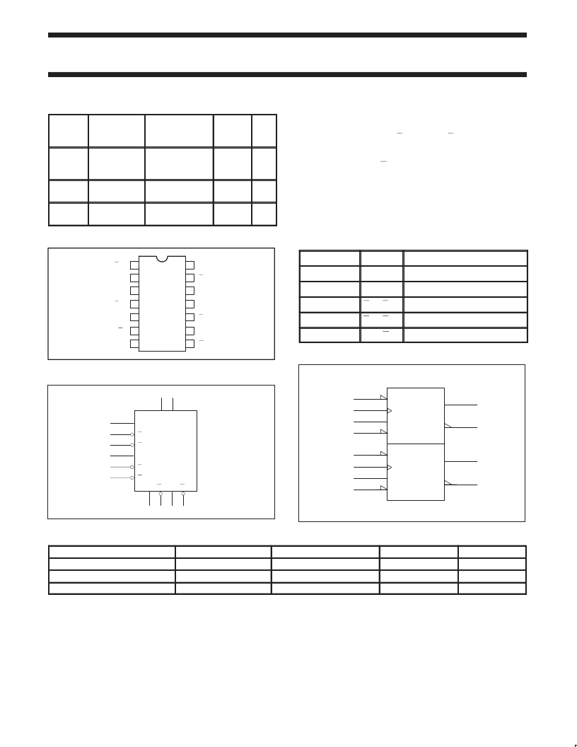
QUICK REFERENCE DATA
SYMBOL
PARAMETER
CONDITIONS
T
amb
= 25
°
C;
GND = 0V
TYPICAL
UNIT
t
PLH
t
PHL
Propagation
delay
CPn to Qn
C
L
= 50pF;
V
CC
= 3.3V
3.1
3.6
ns
C
IN
Input
capacitance
V
I
= 0V or 3.0V
3
pF
I
CC
Total supply
current
V
CC
= 3.6V
0.5
mA
PIN CONFIGURATION
14
13
12
11
10
9
8
7
6
5
4
3
2
1
GND
V
CC
SD1
Q1
Q1
CP1
RD1
D1
RD0
D0
Q0
CP0
SD0
Q0
SF00045
LOGIC SYMBOL
Q0 Q0 Q1 Q1
5
6
9
8
V
= Pin 14
GND = Pin 7
3
4
1
11
10
13
CP0
SD0
RD0
CP1
SD1
RD1
D0
D1
2
12
SA00359
DESCRIPTION
The 74LVT74 is a dual positive edge-triggered D-type flip-flop
featuring individual data, clock, set, and reset inputs; also true and
complementary outputs. Set (SD) and reset (RD) are asynchronous
active low inputs and operate independently of the clock input.
When set and reset are inactive (high), data at the D input is
transferred to the Q and Q outputs on the low-to-high transition of
the clock. Data must be stable just one setup time prior to the
low-to-high transition of the clock for predictable operation. Clock
triggering occurs at a voltage level and is not directly related to the
transition time of the positive-going pulse. Following the hold time
interval, data at the D input may be changed without affecting the
levels of the output.
PIN DESCRIPTION
PIN NUMBER
SYMBOL
NAME AND FUNCTION
2, 12
D0, D1
Data inputs
3, 11
CP0, CP1
Clock inputs (active rising edge)
4, 10
SD0, SD1
Set inputs (active LOW)
1, 13
RD0, RD1
Reset inputs (active LOW)
5, 6, 8, 9
Qn, Qn
Data outputs
LOGIC SYMBOL (IEEE/IEC)
4
3
2
1
10
11
12
13
5
6
9
8
&
S
S
C1
C2
R
1D
2D
R
SF00047
ORDERING INFORMATION
PACKAGES
14-Pin Plastic SO
14-Pin Plastic SSOP
14-Pin Plastic TSSOP
TEMPERATURE RANGE
–40
°
C to +85
°
C
–40
°
C to +85
°
C
–40
°
C to +85
°
C
OUTSIDE NORTH AMERICA
74LVT74 D
74LVT74 DB
74LVT74 PW
NORTH AMERICA
74LVT74 D
74LVT74 DB
74LVT74PW DH
DWG NUMBER
SOT108-1
SOT337-1
SOT402-1
相關PDF資料 |
PDF描述 |
|---|---|
| 74LVT86 | 3.3V Quad 2-input exclusive-OR gate |
| 74LVT86D | 8-Bit Shift Registers With 3-State Output Registers 16-SOIC -40 to 85 |
| 74LVT86DB | 8-Bit Shift Registers With 3-State Output Registers 16-SSOP -40 to 85 |
| 74LVT86PW | 3.3V Quad 2-input exclusive-OR gate |
| 74LVT86PWDH | 3.3V Quad 2-input exclusive-OR gate |
相關代理商/技術(shù)參數(shù) |
參數(shù)描述 |
|---|---|
| 74LVT74PW-T | 功能描述:觸發(fā)器 3.3V DUAL D-TYPE RoHS:否 制造商:Texas Instruments 電路數(shù)量:2 邏輯系列:SN74 邏輯類型:D-Type Flip-Flop 極性:Inverting, Non-Inverting 輸入類型:CMOS 輸出類型: 傳播延遲時間:4.4 ns 高電平輸出電流:- 16 mA 低電平輸出電流:16 mA 電源電壓-最大:5.5 V 最大工作溫度:+ 85 C 安裝風格:SMD/SMT 封裝 / 箱體:X2SON-8 封裝:Reel |
| 74LVT86D,112 | 功能描述:邏輯門 3.3V QUAD 2-INPUT EXC-OR GATE RoHS:否 制造商:Texas Instruments 產(chǎn)品:OR 邏輯系列:LVC 柵極數(shù)量:2 線路數(shù)量(輸入/輸出):2 / 1 高電平輸出電流:- 16 mA 低電平輸出電流:16 mA 傳播延遲時間:3.8 ns 電源電壓-最大:5.5 V 電源電壓-最小:1.65 V 最大工作溫度:+ 125 C 安裝風格:SMD/SMT 封裝 / 箱體:DCU-8 封裝:Reel |
| 74LVT86D,118 | 功能描述:邏輯門 3.3V QUAD 2-INPUT EXC-OR GATE RoHS:否 制造商:Texas Instruments 產(chǎn)品:OR 邏輯系列:LVC 柵極數(shù)量:2 線路數(shù)量(輸入/輸出):2 / 1 高電平輸出電流:- 16 mA 低電平輸出電流:16 mA 傳播延遲時間:3.8 ns 電源電壓-最大:5.5 V 電源電壓-最小:1.65 V 最大工作溫度:+ 125 C 安裝風格:SMD/SMT 封裝 / 箱體:DCU-8 封裝:Reel |
| 74LVT86DB,112 | 功能描述:邏輯門 3.3V QUAD 2-INPUT EXC-OR GATE RoHS:否 制造商:Texas Instruments 產(chǎn)品:OR 邏輯系列:LVC 柵極數(shù)量:2 線路數(shù)量(輸入/輸出):2 / 1 高電平輸出電流:- 16 mA 低電平輸出電流:16 mA 傳播延遲時間:3.8 ns 電源電壓-最大:5.5 V 電源電壓-最小:1.65 V 最大工作溫度:+ 125 C 安裝風格:SMD/SMT 封裝 / 箱體:DCU-8 封裝:Reel |
| 74LVT86DB,118 | 功能描述:邏輯門 3.3V QUAD 2-INPUT EXC-OR GATE RoHS:否 制造商:Texas Instruments 產(chǎn)品:OR 邏輯系列:LVC 柵極數(shù)量:2 線路數(shù)量(輸入/輸出):2 / 1 高電平輸出電流:- 16 mA 低電平輸出電流:16 mA 傳播延遲時間:3.8 ns 電源電壓-最大:5.5 V 電源電壓-最小:1.65 V 最大工作溫度:+ 125 C 安裝風格:SMD/SMT 封裝 / 箱體:DCU-8 封裝:Reel |
發(fā)布緊急采購,3分鐘左右您將得到回復。