- 您現(xiàn)在的位置:買賣IC網(wǎng) > PDF目錄360487 > 74LV27 (NXP Semiconductors N.V.) Triple 3-input NOR gate PDF資料下載
參數(shù)資料
| 型號: | 74LV27 |
| 廠商: | NXP Semiconductors N.V. |
| 英文描述: | Triple 3-input NOR gate |
| 中文描述: | 三3輸入或非門 |
| 文件頁數(shù): | 4/10頁 |
| 文件大小: | 114K |
| 代理商: | 74LV27 |
Philips Semiconductors
Product specification
74LV27
Triple 3-input NOR gate
1998 Apr 20
4
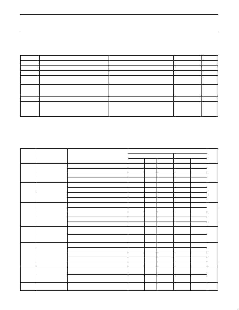
ABSOLUTE MAXIMUM RATINGS
1, 2
In accordance with the Absolute Maximum Rating System (IEC 134).
Voltages are referenced to GND (ground = 0V).
SYMBOL
PARAMETER
V
CC
DC supply voltage
I
IK
DC input diode current
I
OK
DC output diode current
DC output source or sink current
– standard outputs
CONDITIONS
RATING
–0.5 to +7.0
20
50
UNIT
V
mA
mA
V
I
< –0.5 or V
I
> V
CC
+ 0.5V
V
O
< –0.5 or V
O
> V
CC
+ 0.5V
I
O
–0.5V < V
O
< V
CC
+ 0.5V
25
mA
I
GND
,
I
CC
T
stg
DC V
CC
or GND current for types with
– standard outputs
50
mA
Storage temperature range
Power dissipation per package
– plastic DIL
– plastic mini-pack (SO)
– plastic shrink mini-pack (SSOP and TSSOP)
–65 to +150
°
C
P
TOT
for temperature range: –40 to +125
°
C
above +70
°
C derate linearly with 12 mW/K
above +70
°
C derate linearly with 8 mW/K
above +60
°
C derate linearly with 5.5 mW/K
750
500
400
mW
NOTES:
1. Stresses beyond those listed may cause permanent damage to the device. These are stress ratings only and functional operation of the
device at these or any other conditions beyond those indicated under “recommended operating conditions” is not implied. Exposure to
absolute-maximum-rated conditions for extended periods may affect device reliability.
2. The input and output voltage ratings may be exceeded if the input and output current ratings are observed.
DC ELECTRICAL CHARACTERISTICS
Over recommended operating conditions. Voltages are referenced to GND (ground = 0V).
LIMITS
SYMBOL
PARAMETER
TEST CONDITIONS
-40
°
C to +85
°
C
TYP
1
-40
°
C to +125
°
C
MIN
0.9
1.4
2.0
0.7
V
CC
UNIT
MIN
0.9
1.4
2.0
MAX
MAX
V
CC
= 1.2V
V
CC
= 2.0V
V
CC
= 2.7 to 3.6V
V
CC
= 4.5 to 5.5V
V
CC
= 1.2V
V
CC
= 2.0V
V
CC
= 2.7 to 3.6V
V
CC
= 4.5 to 5.5
V
CC
= 1.2V; V
I
= V
IH
or V
IL;
–I
O
= 100
μ
A
V
CC
= 2.0V; V
I
= V
IH
or V
IL;
–I
O
= 100
μ
A
V
CC
= 2.7V; V
I
= V
IH
or V
IL;
–I
O
= 100
μ
A
V
CC
= 3.0V; V
I
= V
IH
or V
IL;
–I
O
= 100
μ
A
V
CC
= 4.5V; V
I
= V
IH
or V
IL;
–I
O
= 100
μ
A
V
IH
HIGH level Input
voltage
V
0.7
V
CC
0.3
0.6
0.8
0.3
0.6
0.8
V
IL
LOW level Input
voltage
V
0.3
V
CC
0.3
V
CC
1.2
2.0
2.7
3.0
4.5
HIGH level output
voltage; all outputs
voltage all out uts
1.8
2.5
2.8
4.3
1.8
2.5
2.8
4.3
V
OH
V
V
OH
HIGH level output
voltage;
STANDARD
outputs
V
CC
= 3.0V; V
I
= V
IH
or V
IL;
–I
O
= 6mA
2.40
2.82
2.20
V
V
CC
= 4.5V; V
I
= V
IH
or V
IL;
–I
O
= 12mA
3.60
4.20
3.50
V
CC
= 1.2V; V
I
= V
IH
or V
IL;
I
O
= 100
μ
A
V
CC
= 2.0V; V
I
= V
IH
or V
IL;
I
O
= 100
μ
A
V
CC
= 2.7V; V
I
= V
IH
or V
IL;
I
O
= 100
μ
A
V
CC
= 3.0V; V
I
= V
IH
or V
IL;
I
O
= 100
μ
A
V
CC
= 4.5V; V
I
= V
IH
or V
IL;
I
O
= 100
μ
A
0
0
0
0
0
LOW level output
voltage; all outputs
voltage all out uts
0.2
0.2
0.2
0.2
0.2
0.2
0.2
0.2
V
OL
V
V
OL
LOW level output
voltage;
STANDARD
outputs
V
CC
= 3.0V; V
I
= V
IH
or V
IL;
I
O
= 6mA
0.25
0.40
0.50
V
V
CC
= 4.5V; V
I
= V
IH
or V
IL;
I
O
= 12mA
0.35
0.55
0.65
I
I
Input leakage
current
V
CC
= 5.5V; V
I
= V
CC
or GND
1.0
1.0
μ
A
相關(guān)PDF資料 |
PDF描述 |
|---|---|
| 74LV27PW | Triple 3-input NOR gate |
| 74LV27PWDH | Triple 3-input NOR gate |
| 74LV27N | Triple 3-input NOR gate |
| 74LV30D | 2K, 256 X 8 SERIAL EE, 1.8V IND, -40C to +85C, 8-TSSOP, TUBE |
| 74LV30DB | 2K, 256 X8 SERIAL EE, 1.8V, -40C to +85C, 8-DFN, T/R |
相關(guān)代理商/技術(shù)參數(shù) |
參數(shù)描述 |
|---|---|
| 74LV273 | 制造商:PHILIPS 制造商全稱:NXP Semiconductors 功能描述:Octal D-type flip-flop with reset; positive-edge trigger |
| 74LV273AFPEL-E | 制造商:Renesas 功能描述:Flip Flop D-Type Bus Interface Pos-Edge 1-Element 20-Pin SOP T/R |
| 74LV273ATELL-E | 制造商:Renesas 功能描述:Flip Flop D-Type Bus Interface Pos-Edge 1-Element 20-Pin TSSOP T/R |
| 74LV273D | 功能描述:觸發(fā)器 3.3V D-TYPE W/RESET POS RoHS:否 制造商:Texas Instruments 電路數(shù)量:2 邏輯系列:SN74 邏輯類型:D-Type Flip-Flop 極性:Inverting, Non-Inverting 輸入類型:CMOS 輸出類型: 傳播延遲時間:4.4 ns 高電平輸出電流:- 16 mA 低電平輸出電流:16 mA 電源電壓-最大:5.5 V 最大工作溫度:+ 85 C 安裝風(fēng)格:SMD/SMT 封裝 / 箱體:X2SON-8 封裝:Reel |
| 74LV273D,112 | 功能描述:觸發(fā)器 3.3V D-TYPE W/RESET RoHS:否 制造商:Texas Instruments 電路數(shù)量:2 邏輯系列:SN74 邏輯類型:D-Type Flip-Flop 極性:Inverting, Non-Inverting 輸入類型:CMOS 輸出類型: 傳播延遲時間:4.4 ns 高電平輸出電流:- 16 mA 低電平輸出電流:16 mA 電源電壓-最大:5.5 V 最大工作溫度:+ 85 C 安裝風(fēng)格:SMD/SMT 封裝 / 箱體:X2SON-8 封裝:Reel |
發(fā)布緊急采購,3分鐘左右您將得到回復(fù)。