- 您現(xiàn)在的位置:買賣IC網(wǎng) > PDF目錄360483 > 74LV03N (NXP SEMICONDUCTORS) Quad 2-input NAND gate PDF資料下載
參數(shù)資料
| 型號: | 74LV03N |
| 廠商: | NXP SEMICONDUCTORS |
| 元件分類: | 通用總線功能 |
| 英文描述: | Quad 2-input NAND gate |
| 中文描述: | LV/LV-A/LVX/H SERIES, QUAD 2-INPUT NAND GATE, PDIP14 |
| 文件頁數(shù): | 2/12頁 |
| 文件大?。?/td> | 119K |
| 代理商: | 74LV03N |
Philips Semiconductors
Product specification
74LV03
Quad 2-input NAND gate
2
1998 Apr 20
853–1963 19257
FEATURES
Wide operating voltage: 1.0 to 5.5V
Optimized for Low Voltage applications: 1.0 to 3.6V
Accepts TTL input levels between V
CC
= 2.7V and V
CC
= 3.6V
Typical V
OLP
(output ground bounce)
T
amb
= 25
°
C
Typical V
OHV
(output V
OH
undershoot)
T
amb
= 25
°
C
Level shifter capability
Output capability: standard (open drain)
I
CC
category: SSI
0.8V @ V
CC
= 3.3V,
2V @ V
CC
= 3.3V,
DESCRIPTION
The 74LV03 is a low–voltage Si–gate CMOS device and is pin and
function compatible with 74HC/HCT03.
The 74LV03 provides the 2–input NAND function.
The 74LV03 has open–drain N–transistor outputs, which are not
clamped by a diode connected to V
CC
. In the OFF–state, i.e. when
one input is LOW, the output may be pulled to any voltage between
GND and V
Omax
. This allows the device to be used as a
LOW–to–HIGH or HIGH–to–LOW level shifter. For digital operation
and OR–tied output applications, these devices must have a pull–up
resistor to establish a logic HIGH level.
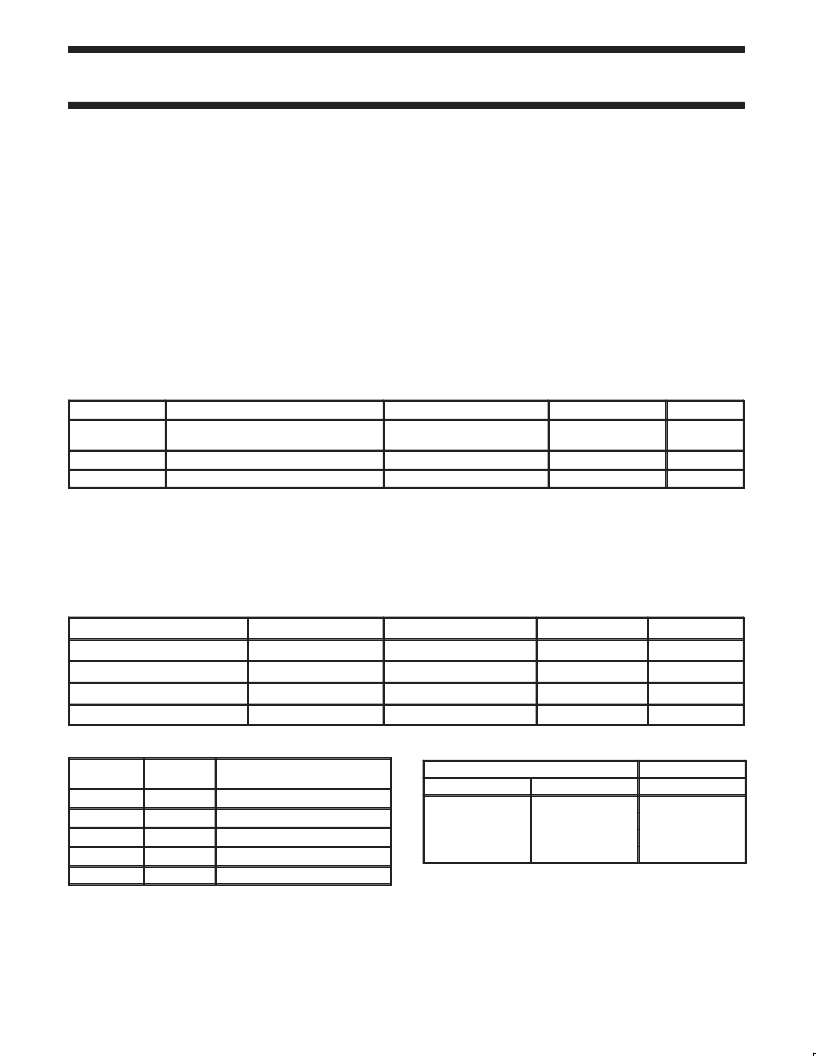
QUICK REFERENCE DATA
GND = 0V; T
amb
= 25
°
C; t
r
=t
f
SYMBOL
2.5 ns
PARAMETER
CONDITIONS
TYPICAL
UNIT
t
PZL
/t
PLZ
Propagation delay
nA, nB to nY
C
L
= 15pF
V
CC
= 3.3V
8
ns
C
I
C
PD
NOTES:
1
C
PD
is used to determine the dynamic power dissipation (P
D
in
μ
W)
P
D
= C
PD
V
CC2
x f
i
(C
L
f
i
= input frequency in MHz; C
L
= output load capacitance in pF;
f
o
= output frequency in MHz; V
CC
= supply voltage in V;
(C
L
V
CC2
f
o
) = sum of the outputs.
2
The condition is V
I
= GND to V
CC
3
The given value of C
PD
is obtained with : C
L
= 0 pF and R
L
=
∞
Input capacitance
3.5
pF
Power dissipation capacitance per gate
Notes 1, 2
4
pF
V
CC2
f
o
) where:
PACKAGES
TEMPERATURE RANGE
OUTSIDE NORTH AMERICA
NORTH AMERICA
PKG. DWG. #
14-Pin Plastic DIL
–40
°
C to +125
°
C
74LV03 N
74LV03 N
SOT27-1
14-Pin Plastic SO
–40
°
C to +125
°
C
74LV03 D
74LV03 D
SOT108-1
14-Pin Plastic SSOP Type II
–40
°
C to +125
°
C
74LV03 DB
74LV03 DB
SOT337-1
14-Pin Plastic TSSOP Type I
–40
°
C to +125
°
C
74LV03 PW
74LV03PW DH
SOT402-1
PIN DESCRIPTION
PIN
NUMBER
SYMBOL
FUNCTION
1, 4, 9, 12
1A to 4A
Data inputs
2, 5, 10, 13
1B to 4B
Data inputs
3, 6, 8, 11
1Y to 4Y
Data outputs
7
GND
Ground (0V)
14
V
CC
Positive supply voltage
FUNCTION TABLE
INPUTS
OUTPUT
nY
Z
Z
Z
L
nA
L
L
H
H
nB
L
H
L
H
NOTES:
H = HIGH voltage level
L = LOW voltage level
Z = High impedance OFF-state
相關(guān)PDF資料 |
PDF描述 |
|---|---|
| 74LV03PW | BREAKOUT TEST CABLE ASSEMBLY; BNC MALE TO INSULATED SPADE LUGS; APPROX. 6" LONG RED & BLACK LEADS |
| 74LV03PWDH | Quad 2-input NAND gate |
| 74LV04PWDH | CERAMIC CHIP/MIL-PRF-55681 |
| 74LV04 | CERAMIC CHIP/MIL-PRF-55681 |
| 74LV08PWDH | Quad 2-input AND gate |
相關(guān)代理商/技術(shù)參數(shù) |
參數(shù)描述 |
|---|---|
| 74LV03PW | 制造商:PHILIPS 制造商全稱:NXP Semiconductors 功能描述:Quad 2-input NAND gate |
| 74LV03PWDH | 制造商:PHILIPS 制造商全稱:NXP Semiconductors 功能描述:Quad 2-input NAND gate |
| 74LV03PW-T | 制造商:未知廠家 制造商全稱:未知廠家 功能描述:Quad 2-input NAND Gate |
| 74LV04 | 制造商:PHILIPS 制造商全稱:NXP Semiconductors 功能描述:Hex inverter |
| 74LV0451D | 制造商:未知廠家 制造商全稱:未知廠家 功能描述:Interface IC |
發(fā)布緊急采購,3分鐘左右您將得到回復(fù)。