- 您現(xiàn)在的位置:買賣IC網(wǎng) > PDF目錄360474 > 74HCT (NXP Semiconductors N.V.) HCMOS family characteristics PDF資料下載
參數(shù)資料
| 型號: | 74HCT |
| 廠商: | NXP Semiconductors N.V. |
| 英文描述: | HCMOS family characteristics |
| 中文描述: | HCMOS家庭特征 |
| 文件頁數(shù): | 2/19頁 |
| 文件大?。?/td> | 88K |
| 代理商: | 74HCT |
March 1988
2
Philips Semiconductors
HCMOS family characteristics
FAMILY
SPECIFICATIONS
GENERAL
These family specifications cover the common electrical
ratings and characteristics of the entire HCMOS
74HC/HCT/HCU family, unless otherwise specified in the
individual device data sheet.
INTRODUCTION
The 74HC/HCT/HCU high-speed Si-gate CMOS logic
family combines the low power advantages of the
HE4000B family with the high speed and drive capability of
the low power Schottky TTL (LSTTL).
The family will have the same pin-out as the 74 series and
provide the same circuit functions.
In these families are included several HE4000B family
circuits which do not have TTL counterparts, and some
special circuits.
The basic family of buffered devices, designated as
XX74HCXXXXX, will operate at CMOS input logic levels
for high noise immunity, negligible typical quiescent supply
and input current. It is operated from a power supply of
2 to 6 V.
A subset of the family, designated as XX74HCTXXXXX,
with the same features and functions as the “HC-types”,
will operate at standard TTL power supply voltage
(5 V
±
10%) and logic input levels (0.8 to 2.0 V) for use as
pin-to-pin compatible CMOS replacements to reduce
power consumption without loss of speed. These types are
also suitable for converted switching from TTL to CMOS.
Another subset, the XX74HCUXXXXX, consists of
single-stage unbuffered CMOS compatible devices for
application in RC or crystal controlled oscillators and other
types of feedback circuits which operate in the linear
mode.
HANDLING MOS DEVICES
Inputs and outputs are protected against electrostatic
effects in a wide variety of device-handling situations.
However, to be totally safe, it is desirable to take handling
precautions into account
(see also “HANDLING PRECAUTIONS”).
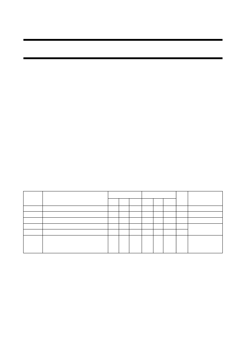
RECOMMENDED OPERATING CONDITIONS FOR 74HC/HCT
Note
1.
For analog switches, e.g. “4016”, “4051 series”, “4351 series”, “4066” and “4067”, the specified maximum operating
supply voltage is 10 V.
SYMBOL PARAMETER
74HC
74HCT
UNIT CONDITIONS
min. typ.
max.
min.
typ.
max.
V
CC
V
I
V
O
T
amb
T
amb
t
r
, t
f
DC supply voltage
DC input voltage range
DC output voltage range
operating ambient temperature range
40
operating ambient temperature range
40
input rise and fall times except for
Schmitt-trigger inputs
2.0
0
0
5.0
6.0
V
CC
V
CC
+
85
+
125
1000
500
400
4.5
0
0
40
40
5.0
5.5
V
CC
V
CC
+
85
+
125
V
V
V
°
C
°
C
see DC and AC
CHAR. per device
6.0
6.0
500
ns
V
CC
= 2.0 V
V
CC
= 4.5 V
V
CC
= 6.0 V
相關(guān)PDF資料 |
PDF描述 |
|---|---|
| 74HCU | HCMOS family characteristics |
| 74HCU04D-T | CERAMIC CHIP/MIL-PRF-55681 |
| 74HCU04 | CERAMIC CHIP/MIL-PRF-55681 |
| 74HCU147N | 10-TO-4 LINE PRIORITY ENCODER |
| 74HCMOS147N | 10-TO-4 LINE PRIORITY ENCODER |
相關(guān)代理商/技術(shù)參數(shù) |
參數(shù)描述 |
|---|---|
| 74HCT00 | 制造商:HAR 功能描述:74HCT00 制造商:NTE Electronics 功能描述: |
| 74HCT00AN | 制造商:AVX Corporation 功能描述: |
| 74HCT00BQ | 制造商:NXP Semiconductors 功能描述:IC QUAD 2 I/P NAND GATE 14-D |
| 74HCT00BQ,115 | 功能描述:邏輯門 QUAD 2-INPUT NAND RoHS:否 制造商:Texas Instruments 產(chǎn)品:OR 邏輯系列:LVC 柵極數(shù)量:2 線路數(shù)量(輸入/輸出):2 / 1 高電平輸出電流:- 16 mA 低電平輸出電流:16 mA 傳播延遲時間:3.8 ns 電源電壓-最大:5.5 V 電源電壓-最小:1.65 V 最大工作溫度:+ 125 C 安裝風(fēng)格:SMD/SMT 封裝 / 箱體:DCU-8 封裝:Reel |
| 74HCT00BQ-G | 功能描述:邏輯門 QUAD 2-INPUT NAND RoHS:否 制造商:Texas Instruments 產(chǎn)品:OR 邏輯系列:LVC 柵極數(shù)量:2 線路數(shù)量(輸入/輸出):2 / 1 高電平輸出電流:- 16 mA 低電平輸出電流:16 mA 傳播延遲時間:3.8 ns 電源電壓-最大:5.5 V 電源電壓-最小:1.65 V 最大工作溫度:+ 125 C 安裝風(fēng)格:SMD/SMT 封裝 / 箱體:DCU-8 封裝:Reel |
發(fā)布緊急采購,3分鐘左右您將得到回復(fù)。