- 您現(xiàn)在的位置:買賣IC網(wǎng) > PDF目錄360466 > 74HCT259 (NXP Semiconductors N.V.) 8-bit addressable latch PDF資料下載
參數(shù)資料
| 型號: | 74HCT259 |
| 廠商: | NXP Semiconductors N.V. |
| 英文描述: | 8-bit addressable latch |
| 中文描述: | 8位可尋址鎖存器 |
| 文件頁數(shù): | 2/11頁 |
| 文件大?。?/td> | 87K |
| 代理商: | 74HCT259 |
December 1990
2
Philips Semiconductors
Product specification
8-bit addressable latch
74HC/HCT259
FEATURES
Combines demultiplexer and 8-bit latch
Serial-to-parallel capability
Output from each storage bit available
Random (addressable) data entry
Easily expandable
Common reset input
Useful as a 3-to-8 active HIGH decoder
Output capability: standard
I
CC
category: MSI
GENERAL DESCRIPTION
The 74HC/HCT259 are high-speed Si-gate CMOS devices
and are pin compatible with low power Schottky TTL
(LSTTL). They are specified in compliance with JEDEC
standard no. 7A.
The 74HC/HCT259 are high-speed 8-bit addressable
latches designed for general purpose storage applications
in digital systems. The “259” are multifunctional devices
capable of storing single-line data in eight addressable
latches, and also 3-to-8 decoder and demultiplexer, with
active HIGH outputs (Q
0
to Q
7
), functions are available.
The “259” also incorporates an active LOW common reset
(MR) for resetting all latches, as well as, an active LOW
enable input (LE).
The “259” has four modes of operation as shown in the
mode select table. In the addressable latch mode, data on
the data line (D) is written into the addressed latch. The
addressed latch will follow the data input with all
non-addressed latches remaining in their previous states.
In the memory mode, all latches remain in their previous
states and are unaffected by the data or address inputs.
In the 3-to-8 decoding or demultiplexing mode, the
addressed output follows the state of the D input with all
other outputs in the LOW state. In the reset mode all
outputs are LOW and unaffected by the address (A
0
to A
2
)
and data (D) input. When operating the “259” as an
addressable latch, changing more than one bit of address
could impose a transient-wrong address. Therefore, this
should only be done while in the memory mode. The mode
select table summarizes the operations of the “259”.
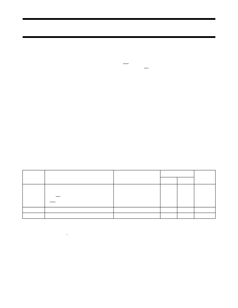
QUICK REFERENCE DATA
GND = 0 V; T
amb
= 25
°
C; t
r
= t
f
= 6 ns
Notes
1.
C
PD
is used to determine the dynamic power dissipation (P
D
in
μ
W):
P
D
= C
PD
×
V
CC2
×
f
i
+ ∑
(C
L
×
V
CC2
×
f
o
) where:
f
i
= input frequency in MHz
f
o
= output frequency in MHz
∑
(C
L
×
V
CC2
×
f
o
) = sum of outputs
C
L
= output load capacitance in pF
V
CC
= supply voltage in V
For HC the condition is V
I
= GND to V
CC
For HCT the condition is V
I
= GND to V
CC
1.5 V
2.
SYMBOL
PARAMETER
CONDITIONS
TYPICAL
UNIT
HC
HCT
t
PHL/
t
PLH
propagation delay
D to Q
n
A
n
, LE to Q
n
MR to Q
n
input capacitance
power dissipation capacitance per latch
C
L
= 15 pF; V
CC
= 5 V
18
17
15
3.5
19
20
20
20
3.5
19
ns
ns
ns
pF
pF
t
PHL
C
I
C
PD
notes 1 and 2
相關PDF資料 |
PDF描述 |
|---|---|
| 74HC259 | 8-bit addressable latch |
| 74HCT273 | 8-Bit Parallel-Out Serial Shift Registers 14-SOIC -40 to 85 |
| 74HC273 | Octal D-type flip-flop with reset; positive-edge trigger |
| 74HC273 | Octal D Flip-Flop with Common Clock and Reset |
| 74HCT27 | 8-Bit Parallel-Out Serial Shift Registers 14-SOIC -40 to 85 |
相關代理商/技術參數(shù) |
參數(shù)描述 |
|---|---|
| 74HCT259BQ | 制造商:NXP Semiconductors 功能描述:Cut Tape 制造商:NXP Semiconductors 功能描述:IC 8BIT LATCH ADDRESS DHVQF 制造商:NXP Semiconductors 功能描述:Latch Addressable 8-CH D-Type 16-Pin DHVQFN EP T/R |
| 74HCT259BQ,115 | 功能描述:閉鎖 8-BIT ADDRESSABLE LATCH RoHS:否 制造商:Micrel 電路數(shù)量:1 邏輯類型:CMOS 邏輯系列:TTL 極性:Non-Inverting 輸出線路數(shù)量:9 高電平輸出電流: 低電平輸出電流: 傳播延遲時間: 電源電壓-最大:12 V 電源電壓-最小:5 V 最大工作溫度:+ 85 C 最小工作溫度:- 40 C 封裝 / 箱體:SOIC-16 封裝:Reel |
| 74HCT259BQ-Q100,11 | 制造商:NXP Semiconductors 功能描述:Latch Addressable 8-CH D-Type 16-Pin DHVQFN EP T/R 制造商:NXP Semiconductors 功能描述:74HCT259BQ-Q100/DHVQFN16/REEL7 - Tape and Reel 制造商:NXP Semiconductors 功能描述:IC LATCH 8BIT ADDRESS 16DHVQFN |
| 74HCT259BQ-Q100,115 | 制造商:NXP Semiconductors 功能描述: |
| 74HCT259D | 功能描述:閉鎖 8-BIT ADDRSSBL LATCH RoHS:否 制造商:Micrel 電路數(shù)量:1 邏輯類型:CMOS 邏輯系列:TTL 極性:Non-Inverting 輸出線路數(shù)量:9 高電平輸出電流: 低電平輸出電流: 傳播延遲時間: 電源電壓-最大:12 V 電源電壓-最小:5 V 最大工作溫度:+ 85 C 最小工作溫度:- 40 C 封裝 / 箱體:SOIC-16 封裝:Reel |
發(fā)布緊急采購,3分鐘左右您將得到回復。