- 您現(xiàn)在的位置:買賣IC網(wǎng) > PDF目錄360458 > 74HCT1G86GW-G Single 2-input Exclusive OR (XOR) Gate PDF資料下載
參數(shù)資料
| 型號: | 74HCT1G86GW-G |
| 英文描述: | Single 2-input Exclusive OR (XOR) Gate |
| 中文描述: | 單2輸入異或(XOR)門 |
| 文件頁數(shù): | 4/16頁 |
| 文件大小: | 78K |
| 代理商: | 74HCT1G86GW-G |
2002 May 15
4
Philips Semiconductors
Product specification
Bus buffer/line driver; 3-state
74HC1G126; 74HCT1G126
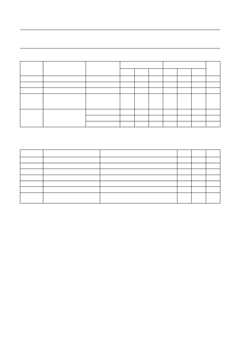
RECOMMENDED OPERATING CONDITIONS
LIMITING VALUES
In accordance with the Absolute Maximum Rating System (IEC 60134); voltages are referenced to GND (ground = 0 V);
notes 1 and 2.
Notes
1.
Stresses beyond those listed may cause permanent damage to the device. These are stress rating only and
functional operation of the device at these or any other conditions beyond those under ‘recommended operating
conditions’ is not implied. Exposure to absolute maximum rated conditions for extended periods may affect device
reliability.
The input and output voltage ratings may be exceeded if the input and output current ratings are observed.
Above 55
°
C the value of P
D
derates linearly with 2.5 mW/K.
2.
3.
SYMBOL
PARAMETER
CONDITIONS
74HC1G
74HCT1G
UNIT
MIN.
TYP.
MAX.
MIN.
TYP.
MAX.
V
CC
V
I
V
O
T
amb
supply voltage
input voltage
output voltage
operating ambient
temperature
2.0
0
0
40
5.0
+25
6.0
V
CC
V
CC
+125
4.5
0
0
40
5.0
+25
5.5
V
CC
V
CC
+125
V
V
V
°
C
see DC and AC
characteristics per
device
V
CC
= 2.0 V
V
CC
= 4.5 V
V
CC
= 6.0 V
t
r
, t
f
input rise and fall times
1000
500
400
500
ns
ns
ns
SYMBOL
PARAMETER
CONDITIONS
MIN.
0.5
65
MAX.
UNIT
V
CC
I
IK
I
OK
I
O
I
CC
T
stg
P
D
supply voltage
input diode current
output diode current
output source or sink current
V
CC
or GND current
storage temperature
power dissipation per package
+7.0
±
20
±
20
±
35.0
±
70
+150
200
V
mA
mA
mA
mA
°
C
mW
V
I
<
0.5 V or V
I
> V
CC
+ 0.5 V
V
O
<
0.5 V or V
O
> V
CC
+ 0.5 V
0.5 V < V
O
< V
CC
+ 0.5 V
for temperature range from
40 to +125
°
C;
note 3
相關(guān)PDF資料 |
PDF描述 |
|---|---|
| 74HC1G14 | Inverting Schmitt-trigger |
| 74HC1G66 | Bilateral switch |
| 74HC10D-T | Triple 3-input NAND Gate |
| 74HC112D-T | J-K-Type Flip-Flop |
| 74HC11D-T | SC70/µDFN, Single/Dual Low-Voltage, Low-Power µP Reset Circuits |
相關(guān)代理商/技術(shù)參數(shù) |
參數(shù)描述 |
|---|---|
| 74HCT1G86GW-Q100H | 制造商:NXP Semiconductors 功能描述:XOR Gate 1-Element 2-IN CMOS 5-Pin TSSOP T/R 制造商:NXP Semiconductors 功能描述:74HCT1G86GW-Q100/UMT5/REELR// - Tape and Reel 制造商:NXP Semiconductors 功能描述:IC GATE EXCL-OR 2-INPUT 5TSSOP |
| 74HCT1G86GW-R | 功能描述:邏輯門 2-INPUT EX-OR GATE RoHS:否 制造商:Texas Instruments 產(chǎn)品:OR 邏輯系列:LVC 柵極數(shù)量:2 線路數(shù)量(輸入/輸出):2 / 1 高電平輸出電流:- 16 mA 低電平輸出電流:16 mA 傳播延遲時間:3.8 ns 電源電壓-最大:5.5 V 電源電壓-最小:1.65 V 最大工作溫度:+ 125 C 安裝風(fēng)格:SMD/SMT 封裝 / 箱體:DCU-8 封裝:Reel |
| 74HCT20D | 功能描述:邏輯門 DUAL 4-INPUT NAND GATE RoHS:否 制造商:Texas Instruments 產(chǎn)品:OR 邏輯系列:LVC 柵極數(shù)量:2 線路數(shù)量(輸入/輸出):2 / 1 高電平輸出電流:- 16 mA 低電平輸出電流:16 mA 傳播延遲時間:3.8 ns 電源電壓-最大:5.5 V 電源電壓-最小:1.65 V 最大工作溫度:+ 125 C 安裝風(fēng)格:SMD/SMT 封裝 / 箱體:DCU-8 封裝:Reel |
| 74HCT20D,652 | 功能描述:邏輯門 DUAL 4-INPUT NAND RoHS:否 制造商:Texas Instruments 產(chǎn)品:OR 邏輯系列:LVC 柵極數(shù)量:2 線路數(shù)量(輸入/輸出):2 / 1 高電平輸出電流:- 16 mA 低電平輸出電流:16 mA 傳播延遲時間:3.8 ns 電源電壓-最大:5.5 V 電源電壓-最小:1.65 V 最大工作溫度:+ 125 C 安裝風(fēng)格:SMD/SMT 封裝 / 箱體:DCU-8 封裝:Reel |
| 74HCT20D,653 | 功能描述:邏輯門 DUAL 4-INPUT NAND RoHS:否 制造商:Texas Instruments 產(chǎn)品:OR 邏輯系列:LVC 柵極數(shù)量:2 線路數(shù)量(輸入/輸出):2 / 1 高電平輸出電流:- 16 mA 低電平輸出電流:16 mA 傳播延遲時間:3.8 ns 電源電壓-最大:5.5 V 電源電壓-最小:1.65 V 最大工作溫度:+ 125 C 安裝風(fēng)格:SMD/SMT 封裝 / 箱體:DCU-8 封裝:Reel |
發(fā)布緊急采購,3分鐘左右您將得到回復(fù)。