- 您現(xiàn)在的位置:買賣IC網(wǎng) > PDF目錄360426 > 74F1604 (NXP Semiconductors N.V.) Latch PDF資料下載
參數(shù)資料
| 型號: | 74F1604 |
| 廠商: | NXP Semiconductors N.V. |
| 英文描述: | Latch |
| 中文描述: | 鎖存 |
| 文件頁數(shù): | 4/10頁 |
| 文件大?。?/td> | 92K |
| 代理商: | 74F1604 |
Philips Semiconductors
Product specification
74F1604
Latch
October 4, 1990
4
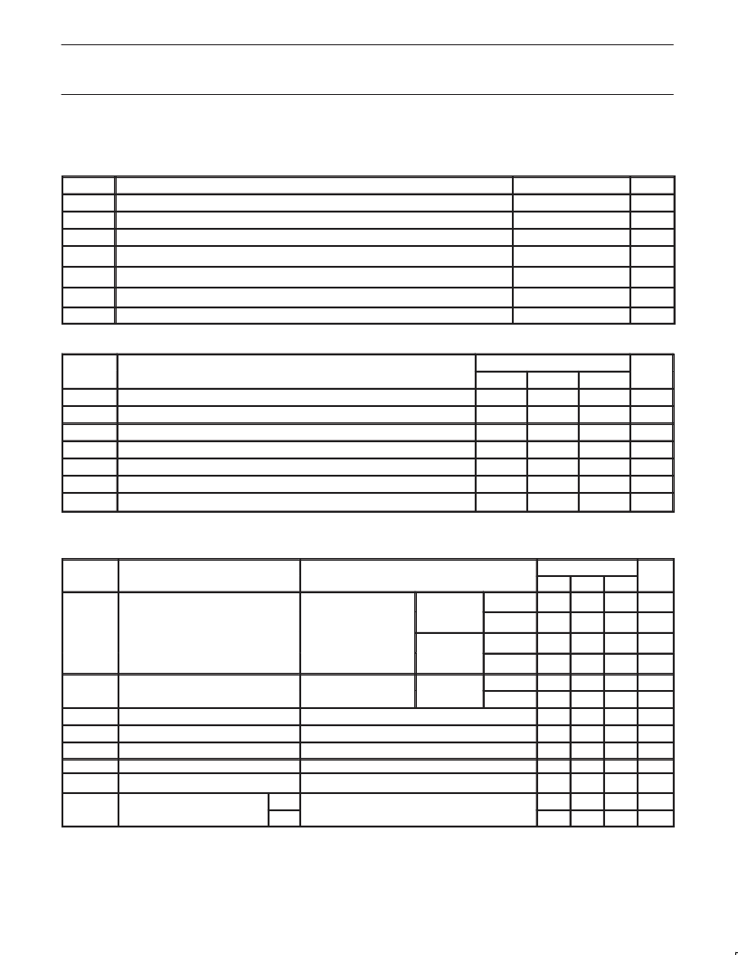
ABSOLUTE MAXIMUM RATINGS
(Operation beyond the limit set forth in this table may impair the useful life of the device.
Unless otherwise noted these limits are over the operating free air temperature range.)
SYMBOL
PARAMETER
RATING
UNIT
V
CC
V
IN
I
IN
V
OUT
Supply voltage
–0.5 to +7.0
V
Input voltage
–0.5 to +7.0
V
Input current
–30 to +5
mA
Voltage applied to output in high output state
–0.5 to V
CC
V
I
OUT
Current applied to output in low output state
40
mA
T
amb
Operating free air temperature range
0 to +70
°
C
°
C
T
stg
Storage temperature range
–65 to +150
RECOMMENDED OPERATING CONDITIONS
SYMBOL
PARAMETER
LIMITS
UNIT
MIN
NOM
MAX
V
CC
V
IH
V
IL
I
Ik
I
OH
I
OL
Supply voltage
4.5
5.0
5.5
V
High–level input voltage
2.0
V
Low–level input voltage
0.8
V
Input clamp current
–18
mA
High–level output current
–1
mA
Low–level output current
20
mA
°
C
T
amb
Operating free air temperature range
0
+70
DC ELECTRICAL CHARACTERISTICS
(Over recommended operating free-air temperature range unless otherwise noted.)
SYMBOL
PARAMETER
TEST
LIMITS
TYP
2
UNIT
CONDITIONS
1
MIN
MAX
I
OH
= –1mA
±
10%V
CC
2.5
V
V
OH
High-level output voltage
V
CC
= MIN, V
IL
= MAX,
±
5%V
CC
2.7
3.4
V
V
IH
= MIN
I
OH
= –3mA
±
10%V
CC
2.4
V
±
5%V
CC
2.7
3.3
V
V
OL
Low-level output voltage
V
CC
= MIN, V
IL
= MAX,
V
IH
= MIN
V
CC
= MIN, I
I
= I
IK
V
CC
= MAX, V
I
= 7.0V
V
CC
= MAX, V
I
= 2.7V
V
CC
= MAX, V
I
= 0.5V
I
OL
= MAX
±
10%V
CC
±
5%V
CC
0.30
0.50
V
0.30
0.50
V
V
IK
I
I
I
IH
I
IL
Input clamp voltage
–0.73
-1.2
V
μ
A
μ
A
μ
A
Input current at maximum input voltage
100
High–level input current
Low–level input current
Short–circuit output current
3
20
–20
I
OS
V
CC
= MAX
-60
-150
mA
I
CC
Supply current (total)
I
CCH
I
CCL
V
CC
= MAX
60
80
mA
75
100
mA
Notes to DC electrical characteristics
1. For conditions shown as MIN or MAX, use the appropriate value specified under recommended operating conditions for the applicable type.
2. All typical values are at V
CC
= 5V, T
amb
= 25
°
C.
3. Not more than one output should be shorted at a time. For testing I
OS
, the use of high-speed test apparatus and/or sample-and-hold
techniques are preferable in order to minimize internal heating and more accurately reflect operational values. Otherwise, prolonged shorting
of a high output may raise the chip temperature well above normal and thereby cause invalid readings in other parameter tests. In any
sequence of parameter tests, I
OS
tests should be performed last.
相關(guān)PDF資料 |
PDF描述 |
|---|---|
| 74F161A | 4-bit binary counters(4位二進制計數(shù)器) |
| 74F163A | 4-bit binary counter |
| 74F163ASCX | Synchronous Up Counter |
| 74F163ASJQR | Synchronous Up Counter |
| 74F163ASJX | Synchronous Up Counter |
相關(guān)代理商/技術(shù)參數(shù) |
參數(shù)描述 |
|---|---|
| 74F160A | 制造商:FAIRCHILD 制造商全稱:Fairchild Semiconductor 功能描述:Synchronous Presettable BCD Decade Counter |
| 74F160A WAF | 制造商:Fairchild Semiconductor Corporation 功能描述: |
| 74F160AD | 制造商:n/a 功能描述:74F160 MOT/SIG S1I2A |
| 74F160ADC | 制造商:Rochester Electronics LLC 功能描述:- Bulk |
| 74F160APC | 功能描述:計數(shù)器 IC Syn BCD Decade Ctr RoHS:否 制造商:NXP Semiconductors 計數(shù)器類型:Binary Counters 邏輯系列:74LV 位數(shù):10 計數(shù)法: 計數(shù)順序: 工作電源電壓:1 V to 5.5 V 工作溫度范圍:- 40 C to + 125 C 封裝 / 箱體:SOT-109 封裝:Reel |
發(fā)布緊急采購,3分鐘左右您將得到回復(fù)。