- 您現(xiàn)在的位置:買賣IC網(wǎng) > PDF目錄360418 > 74AVC16835ADGV BUFFER/DRIVER|SINGLE|18-BIT|AVC/ALVC-CMOS|TSSOP|56PIN|PLASTIC PDF資料下載
參數(shù)資料
| 型號(hào): | 74AVC16835ADGV |
| 英文描述: | BUFFER/DRIVER|SINGLE|18-BIT|AVC/ALVC-CMOS|TSSOP|56PIN|PLASTIC |
| 中文描述: | 緩沖器/驅(qū)動(dòng)器|單|18位|AVC/ALVC-CMOS|TSSOP|56引腳|塑料 |
| 文件頁(yè)數(shù): | 8/10頁(yè) |
| 文件大小: | 102K |
| 代理商: | 74AVC16835ADGV |
Philips Semiconductors
Product specification
74AVC16334A
16-bit registered driver with inverted register enable and
Dynamic Controlled Outputs
(3-State)
2000 Aug 03
8
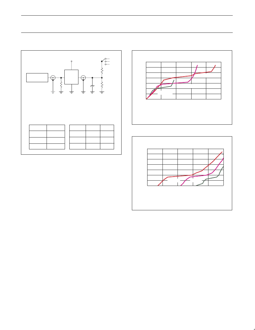
TEST CIRCUIT
SWITCH POSITION
PULSE
GENERATOR
R
T
V
I
D.U.T.
V
O
C
L
V
CC
R
L
Test Circuit for switching times
Open
GND
S
1
DEFINITIONS
R
L
= Load resistor
C
L
= Load capacitance includes jig and probe capacitance
R
T
= Termination resistance should be equal to Z
OUT
of pulse generators.
V
CC
V
I
< 2.3 V
V
CC
TEST
S
1
t
PLH/
t
PHL
Open
2
V
CC
t
PLZ/
t
PZL
V
CC
2.3–2.7 V
t
PHZ/
t
PZH
GND
R
L
2 * V
CC
SV01018
R
L
1000
500
V
CC
3.0 V
500
Waveform 7.
Load circuitry for switching times
GRAPHS
SH00204
0
0.5
1
1.5
2
2.5
3
3.5
0
50
100
150
200
250
OUTPUT CURRENT (mA)
O
V
= 3.3 V
VCC
= 2.5 V
VCC
VCC = 1.8 V
IOL
Figure 1. Output voltage (V
OL
) vs. output current (I
OL
)
SH00205
–250
–200
–150
–100
–50
0
0.0
0.5
1.0
1.5
2.0
2.5
3.0
3.5
= 3.3 V
= 2.5 V
= 1.8 V
OUTPUT CURRENT (mA)
O
V
VCC
IOH
VCC
VCC
Figure 2. Output voltage (V
OH
) vs. output current (I
OH
)
A Dynamic Controlled Output (DCO) circuit is designed in. During
the transition, it initially lowers the output impedance to effectively
drive the load and, subsequently, raises the impedance to reduce
noise. Figures 1 and 2 show V
OL
vs. I
OL
and V
OH
vs. I
OH
curves to
illustrate the output impedance and drive capability of the circuit. At
the beginning of the signal transition, the DCO circuit provides a
maximum dynamic drive that is equivalent to a high drive standard
output device.
相關(guān)PDF資料 |
PDF描述 |
|---|---|
| 74AVC16836A | 20-bit registered driver with inverted register enable and Dynamic Controlled Outputs(TM) (3-State) |
| 74AVC16836ADGG | 20-Bit Buffer/Driver |
| 74AVC16836ADGV | Buffer/Driver |
| 74AVCH16245DGG | BUS TRANSCEIVER|DUAL|8-BIT|AVC/ALVC-CMOS|TSSOP|48PIN|PLASTIC |
| 74AVC16373 | 16-bit D-type transparent latch; 3.6 V tolerant; 3-state |
相關(guān)代理商/技術(shù)參數(shù) |
參數(shù)描述 |
|---|---|
| 74AVC16835ADGV,112 | 功能描述:總線收發(fā)器 18-BIT REG DRIVER-DC RoHS:否 制造商:Fairchild Semiconductor 邏輯類型:CMOS 邏輯系列:74VCX 每芯片的通道數(shù)量:16 輸入電平:CMOS 輸出電平:CMOS 輸出類型:3-State 高電平輸出電流:- 24 mA 低電平輸出電流:24 mA 傳播延遲時(shí)間:6.2 ns 電源電壓-最大:2.7 V, 3.6 V 電源電壓-最小:1.65 V, 2.3 V 最大工作溫度:+ 85 C 封裝 / 箱體:TSSOP-48 封裝:Reel |
| 74AVC16835ADGV,118 | 功能描述:總線收發(fā)器 18-BIT REG DRIVER-DC RoHS:否 制造商:Fairchild Semiconductor 邏輯類型:CMOS 邏輯系列:74VCX 每芯片的通道數(shù)量:16 輸入電平:CMOS 輸出電平:CMOS 輸出類型:3-State 高電平輸出電流:- 24 mA 低電平輸出電流:24 mA 傳播延遲時(shí)間:6.2 ns 電源電壓-最大:2.7 V, 3.6 V 電源電壓-最小:1.65 V, 2.3 V 最大工作溫度:+ 85 C 封裝 / 箱體:TSSOP-48 封裝:Reel |
| 74AVC16835ADGV-T | 功能描述:總線收發(fā)器 18-BIT REG DRIVER-DC OUTPUT 3S RoHS:否 制造商:Fairchild Semiconductor 邏輯類型:CMOS 邏輯系列:74VCX 每芯片的通道數(shù)量:16 輸入電平:CMOS 輸出電平:CMOS 輸出類型:3-State 高電平輸出電流:- 24 mA 低電平輸出電流:24 mA 傳播延遲時(shí)間:6.2 ns 電源電壓-最大:2.7 V, 3.6 V 電源電壓-最小:1.65 V, 2.3 V 最大工作溫度:+ 85 C 封裝 / 箱體:TSSOP-48 封裝:Reel |
| 74AVC16835DGG | 制造商:PHILIPS 制造商全稱:NXP Semiconductors 功能描述:18-bit registered driver 3-State |
| 74AVC16835DGGRE4 | 功能描述:通用總線函數(shù) 18B Univ Bus Driver RoHS:否 制造商:Texas Instruments 邏輯類型:CMOS 邏輯系列:74VMEH 電路數(shù)量:1 開啟電阻(最大值): 傳播延遲時(shí)間:10.1 ns 電源電壓-最大:3.45 V 電源電壓-最小:3.15 V 最大工作溫度:+ 85 C 最小工作溫度:0 C 封裝 / 箱體:TSSOP-48 封裝:Reel |
發(fā)布緊急采購(gòu),3分鐘左右您將得到回復(fù)。