- 您現(xiàn)在的位置:買賣IC網(wǎng) > PDF目錄360413 > 74ALVC16540DGG Dual 8-Bit Buffer/Driver PDF資料下載
參數(shù)資料
| 型號: | 74ALVC16540DGG |
| 英文描述: | Dual 8-Bit Buffer/Driver |
| 中文描述: | 雙8位緩沖器/驅(qū)動器 |
| 文件頁數(shù): | 2/5頁 |
| 文件大小: | 53K |
| 代理商: | 74ALVC16540DGG |
www.fairchildsemi.com
2
7
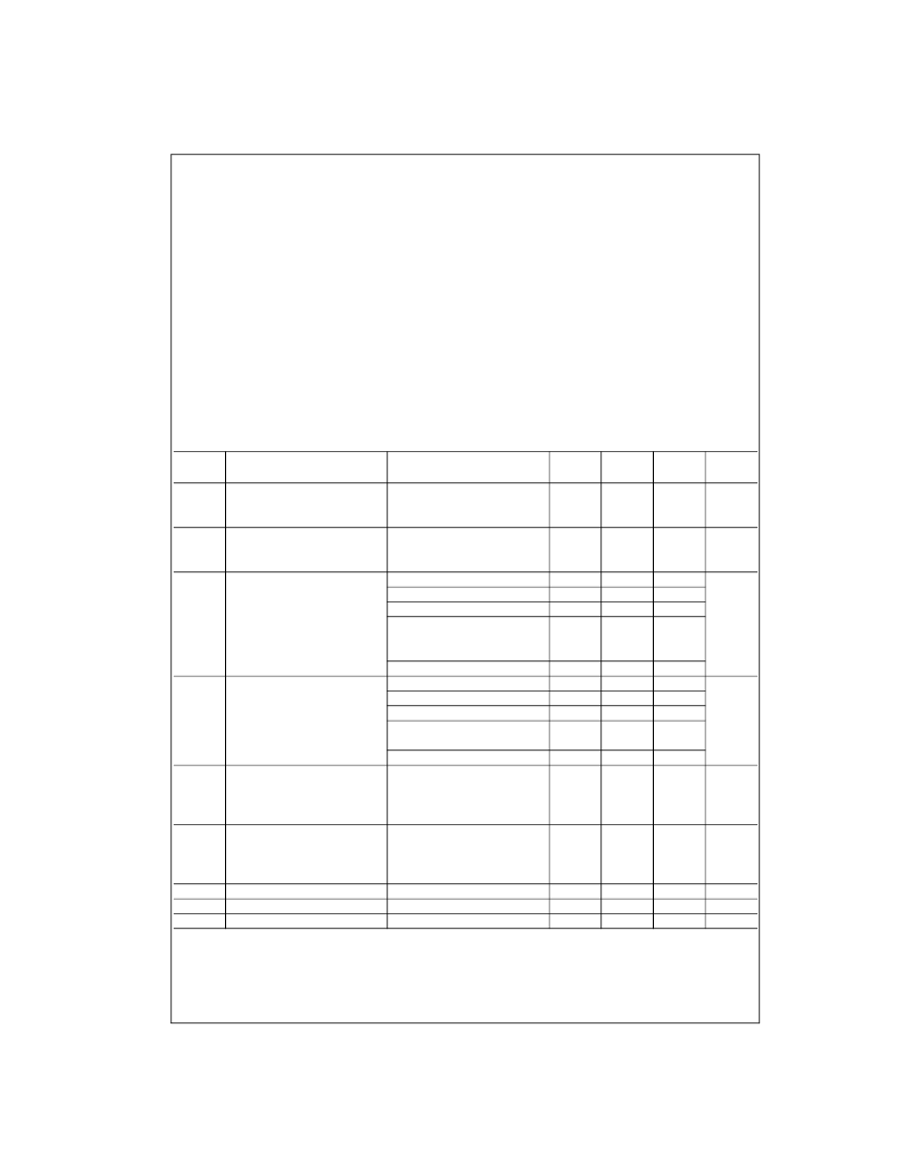
Absolute Maximum Ratings
(Note 1)
Recommended Operating
Conditions
(Note 3)
Note 1:
The Absolute Maximum Ratings are those values beyond which
the safety of the device cannot be guaranteed. The device should not be
operated at these limits. The parametric values defined in the Electrical
Characteristics tables are not guaranteed at the Absolute Maximum Rat-
ings. The
“
Recommended Operating Conditions
”
table will define the condi-
tions for actual device operation.
Note 2:
I
O
Absolute Maximum Rating must be observed, limited to 4.6V.
Note 3:
Floating or unused control inputs must be held HIGH or LOW.
DC Electrical Characteristics
Supply Voltage (V
CC
)
DC Input Voltage (V
I
)
Output Voltage (V
O
) (Note 2)
DC Input Diode Current (I
IK
)
V
I
<
0V
DC Output Diode Current (I
OK
)
V
O
<
0V
DC Output Source/Sink Current
(I
OH
/I
OL
)
DC V
CC
or GND Current per
Supply Pin (I
CC
or GND)
Storage Temperature Range (T
STG
)
0.5V to
+
4.6V
0.5V to 4.6V
0.5V to V
CC
+
0.5V
50 mA
50 mA
±
50 mA
±
100 mA
65
°
C to
+
150
°
C
Power Supply
Operating
Input Voltage (V
I
)
Output Voltage (V
O
)
Free Air Operating Temperature (T
A
)
Minimum Input Edge Rate (
t/
V)
V
IN
=
0.8V to 2.0V, V
CC
=
3.0V
1.65V to 3.6V
0V to V
CC
0V to V
CC
40
°
C to
+
85
°
C
5 ns/V
Symbol
Parameter
Conditions
V
CC
(V)
Min
Max
Units
V
IH
HIGH Level Input Voltage
1.65 - 1.95
2.3 - 2.7
2.7 - 3.6
0.65 x V
CC
1.7
2.0
V
V
IL
LOW Level Input Voltage
1.65 - 1.95
2.3 - 2.7
2.7 - 3.6
0.35 x V
CC
0.7
0.8
V
V
OH
HIGH Level Output Voltage
I
OH
=
100
μ
A
I
OH
=
4 mA
I
OH
=
6 mA
I
OH
=
12 mA
1.65 - 3.6
1.65
2.3
V
CC
- 0.2
1.2
2.0
V
2.3
2.7
3.0
1.7
2.2
2.4
I
OH
=
24 mA
I
OL
=
100
μ
A
I
OL
=
4 mA
I
OL
=
6 mA
I
OL
=
12 mA
3.0
2
V
OL
LOW Level Output Voltage
1.65 - 3.6
1.65
0.2
0.45
V
2.3
2.3
2.7
0.4
0.7
0.4
I
OL
=
24 mA
3.0
1.65
2.3
0.55
4
12
12
24
4
I
OH
High Level Output Current
mA
2.7
3.0
1.65
I
OL
LOW Level Output Current
mA
2.3
2.7
3
12
12
24
±
5.0
10
750
I
I
I
CC
I
CC
Input Leakage Current
Quiescent Supply Current
Increase in I
CC
per Input
0
≤
V
I
≤
3.6V
V
I
=
V
CC
or GND, I
O
=
0
V
IH
=
V
CC
0.6V
3.6
3.6
μ
A
μ
A
μ
A
3 - 3.6
相關(guān)PDF資料 |
PDF描述 |
|---|---|
| 74ALVC16540DL | Dual 8-Bit Buffer/Driver |
| 74ALVC16541DGG | Dual 8-Bit Buffer/Driver |
| 74ALVC16541DL | Dual 8-Bit Buffer/Driver |
| 74ALVC16543DGG | Dual 8-bit Bus Transceiver |
| 74ALVC16543DL | Dual 8-bit Bus Transceiver |
相關(guān)代理商/技術(shù)參數(shù) |
參數(shù)描述 |
|---|---|
| 74ALVC16540DL | 制造商:未知廠家 制造商全稱:未知廠家 功能描述:Dual 8-Bit Buffer/Driver |
| 74ALVC16541DGG | 制造商:未知廠家 制造商全稱:未知廠家 功能描述:Dual 8-Bit Buffer/Driver |
| 74ALVC16541DL | 制造商:未知廠家 制造商全稱:未知廠家 功能描述:Dual 8-Bit Buffer/Driver |
| 74ALVC16543DGG | 制造商:未知廠家 制造商全稱:未知廠家 功能描述:Dual 8-bit Bus Transceiver |
| 74ALVC16543DL | 制造商:未知廠家 制造商全稱:未知廠家 功能描述:Dual 8-bit Bus Transceiver |
發(fā)布緊急采購,3分鐘左右您將得到回復(fù)。