- 您現(xiàn)在的位置:買賣IC網(wǎng) > PDF目錄360413 > 74ALS652 (NXP Semiconductors N.V.) Transceiver/register PDF資料下載
參數(shù)資料
| 型號: | 74ALS652 |
| 廠商: | NXP Semiconductors N.V. |
| 英文描述: | Transceiver/register |
| 中文描述: | 收發(fā)器/注冊 |
| 文件頁數(shù): | 5/13頁 |
| 文件大小: | 156K |
| 代理商: | 74ALS652 |
Philips Semiconductors
Product specification
74ALS651/74ALS651-1
74ALS652/74ALS652-1
Transceiver/register
1991 Feb 08
5
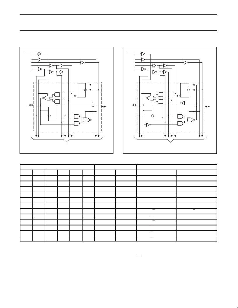
LOGIC DIAGRAM – 74ALS651/651-1
V
=
Pin 24
GND = Pin 12
A0
OEBA
B0
1D
C1
1D
C1
1 OF 8 CHANNELS
TO 7 OTHER CHANNELS
21
4
20
3
23
22
1
2
OEAB
CPBA
SBA
SPAB
SAB
SC00134
LOGIC DIAGRAM – 74ALS652/652-1
V
=
Pin 24
GND = Pin 12
A0
OEBA
B0
1D
C1
1D
C1
1 OF 8 CHANNELS
TO 7 OTHER CHANNELS
21
4
20
3
23
22
1
2
OEAB
CPBA
SBA
SPAB
SAB
SC00135
FUNCTION TABLE
INPUTS
DATA I/O
OPERATING MODE
OEAB
OEBA
CPAB
CPBA
SAB
SBA
An
Bn
74ALS651/74ALS651-1
74ALS652/74ALS652-1
L
H
H or L
H or L
X
X
Input
Input
Isolation
Isolation
L
H
↑
↑
↑
↑
X
X
Input
Input
Store A and B data
Store A and B data
X
H
H or L
X
X
Input
Unspecified*
Store A, hold B
Store A, hold B
H
H
↑
↑
↑
L
X
Input
Output
Store A in both registers
Store A in both registers
L
X
H or L
X
S
Unspecified*
Input
Hold A, store B
Hold A, store B
L
L
↑
X
L
Output
Input
Store B in both registers
Store B in both registers
L
L
X
X
X
L
Output
Input
Real time B data to A bus
Real time B data to A bus
L
L
X
H or L
X
H
Output
Input
Stored B data to A bus
Stored B data to A bus
H
H
X
X
L
X
Input
Output
Real time A data to B bus
Real time A data to B bus
H
H
H or L
X
H
X
Input
Output
Stored A data to B bus
Stored A data to B bus
H
L
H or L
H or L
H
H
Output
Output
Stored A data to B bus
Stored A data to B bus
H
L
H or L
H or L
H
H
Output
Output
Stored B data to A bus
Stored B data to A bus
NOTES:
H =
L
=
X =
*
=
High voltage level
Low voltage level
Don’t care
The data output function may be enabled or disabled by various signals at the OE and DIR inputs. Data input functions are always
enabled, i.e., data at the bus pins will be stored on every Low-to-High transition of the clock.
Low-to-High clock transition
↑
=
相關(guān)PDF資料 |
PDF描述 |
|---|---|
| 74ALS652-1 | Transceiver/register |
| 74ALS652-1D | Transceiver/register |
| 74ALS652-1N | Transceiver/register |
| 74ALS652D | Transceiver/register |
| 74ALS652N | Transceiver/register |
相關(guān)代理商/技術(shù)參數(shù) |
參數(shù)描述 |
|---|---|
| 74ALS652-1 | 制造商:PHILIPS 制造商全稱:NXP Semiconductors 功能描述:Transceiver/register |
| 74ALS652-1D | 制造商:PHILIPS 制造商全稱:NXP Semiconductors 功能描述:Transceiver/register |
| 74ALS652-1N | 制造商:PHILIPS 制造商全稱:NXP Semiconductors 功能描述:Transceiver/register |
| 74ALS652A1NT | 制造商: 功能描述: 制造商:undefined 功能描述: |
| 74ALS652D | 制造商:PHILIPS 制造商全稱:NXP Semiconductors 功能描述:Transceiver/register |
發(fā)布緊急采購,3分鐘左右您將得到回復(fù)。