- 您現(xiàn)在的位置:買賣IC網(wǎng) > PDF目錄360357 > 74ABT573 (Fairchild Semiconductor Corporation) Synchronous 4-Bit Binary Counter 16-SOIC 0 to 70 PDF資料下載
參數(shù)資料
| 型號: | 74ABT573 |
| 廠商: | Fairchild Semiconductor Corporation |
| 元件分類: | 通用總線功能 |
| 英文描述: | Synchronous 4-Bit Binary Counter 16-SOIC 0 to 70 |
| 中文描述: | 八路D類鎖存器與三態(tài)輸出 |
| 文件頁數(shù): | 1/6頁 |
| 文件大?。?/td> | 67K |
| 代理商: | 74ABT573 |
Philips Semiconductors
Product specification
74ABT573A
Octal D-type transparent latch (3-State)
1
1995 Sep 06
853–1455 15703
FEATURES
74ABT573A is flow-through pinout version of 74ABT373
Inputs and outputs on opposite side of package allow easy
interface to microprocessors
3-State output buffers
Common output enable
Latch-up protection exceeds 500mA per JEDEC Std 17
ESD protection exceeds 2000 V per MIL STD 883 Method 3015
and 200 V per Machine Model
Power-up 3-State
Power-up reset
DESCRIPTION
The 74ABT573A high-performance BiCMOS device combines low
static and dynamic power dissipation with high speed and high
output drive.
The 74ABT573A device is an octal transparent latch coupled to
eight 3-State output buffers. The two sections of the device are
controlled independently by Enable (E) and Output Enable (OE)
control gates. The 74ABT573A is functionally identical to the
74ABT373 but has a flow-through pinout configuration to facilitate
PC board layout and allow easy interface with microprocessors.
The data on the D inputs are transferred to the latch outputs when
the Latch Enable (E) input is High. The latch remains transparent to
the data inputs while E is High, and stores the data that is present
one setup time before the High-to-Low enable transition.
The 3-State output buffers are designed to drive heavily loaded
3-State buses, MOS memories, or MOS microprocessors. The
active-Low Output Enable (OE) controls all eight 3-State buffers
independent of the latch operation.
When OE is Low, the latched or transparent data appears at the
outputs. When OE is High, the outputs are in the High-impedance
”O(jiān)FF” state, which means they will neither drive nor load the bus.
QUICK REFERENCE DATA
SYMBOL
PARAMETER
CONDITIONS
T
amb
= 25
°
C; GND = 0V
TYPICAL
UNIT
t
PLH
t
PHL
C
IN
C
OUT
I
CCZ
Propagation delay
Dn to Qn
Input capacitance
Output capacitance
Total supply current
C
L
= 50pF; V
CC
= 5V
2.8
3.3
3
6
100
ns
V
I
= 0V or V
CC
Outputs disabled; V
O
= 0V or V
CC
Outputs disabled; V
CC
=5.5V
pF
pF
μ
A
ORDERING INFORMATION
PACKAGES
20-Pin Plastic DIP
20-Pin plastic SO
20-Pin Plastic SSOP Type II
20-Pin Plastic TSSOP Type I
TEMPERATURE RANGE
–40
°
C to +85
°
C
–40
°
C to +85
°
C
–40
°
C to +85
°
C
–40
°
C to +85
°
C
OUTSIDE NORTH AMERICA
74ABT573A N
74ABT573A D
74ABT573A DB
74ABT573A PW
NORTH AMERICA
74ABT573A N
74ABT573A D
74ABT573A DB
74ABT573APW DH
DWG NUMBER
SOT146-1
SOT163-1
SOT339-1
SOT360-1
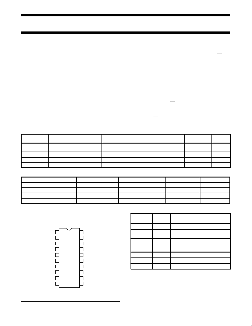
PIN CONFIGURATION
20
19
18
17
16
15
14
13
12
10
11
9
8
7
6
5
4
3
2
1
V
CC
Q0
Q1
Q2
Q3
Q4
Q5
Q6
Q7
E
OE
D0
D1
D2
D3
D4
D5
D6
D7
GND
SA00185
PIN DESCRIPTION
PIN
NUMBER
SYMBOL
FUNCTION
1
OE
Output enable input (active-Low)
2, 3, 4, 5,
6, 7, 8, 9
D0-D7
Data inputs
19, 18, 17,
16, 15, 14,
13, 12
Q0-Q7
Data outputs
11
E
Enable input (active-High)
10
GND
Ground (0V)
20
V
CC
Positive supply voltage
相關(guān)PDF資料 |
PDF描述 |
|---|---|
| 74ABT573CMSA | Synchronous 4-Bit Binary Counter 16-SO 0 to 70 |
| 74ABT573CMTC | Octal D-Type Latch with 3-STATE Outputs |
| 74ABT573CPC | Octal D-Type Latch with 3-STATE Outputs |
| 74ABT573CSC | Octal D-Type Latch with 3-STATE Outputs |
| 74ABT573CSJ | Synchronous 4-Bit Up/Down Binary Counter 16-SOIC 0 to 70 |
相關(guān)代理商/技術(shù)參數(shù) |
參數(shù)描述 |
|---|---|
| 74ABT573_07 | 制造商:FAIRCHILD 制造商全稱:Fairchild Semiconductor 功能描述:Octal D-Type Latch with 3-STATE Outputs |
| 74ABT573_ZAF3026B WAF | 制造商:Fairchild Semiconductor Corporation 功能描述: |
| 74ABT573_ZAF3116B WAF | 制造商:Fairchild Semiconductor Corporation 功能描述: |
| 74ABT573A | 制造商:PHILIPS 制造商全稱:NXP Semiconductors 功能描述:Octal D-type transparent latch 3-State |
| 74ABT573AD | 功能描述:閉鎖 OCTAL D TRANSPARENT LATCH 3-S RoHS:否 制造商:Micrel 電路數(shù)量:1 邏輯類型:CMOS 邏輯系列:TTL 極性:Non-Inverting 輸出線路數(shù)量:9 高電平輸出電流: 低電平輸出電流: 傳播延遲時間: 電源電壓-最大:12 V 電源電壓-最小:5 V 最大工作溫度:+ 85 C 最小工作溫度:- 40 C 封裝 / 箱體:SOIC-16 封裝:Reel |
發(fā)布緊急采購,3分鐘左右您將得到回復。