- 您現(xiàn)在的位置:買賣IC網(wǎng) > PDF目錄360357 > 74ABT5074D (NXP SEMICONDUCTORS) Synchronizing dual D-type flip-flop with metastable immune characteristics PDF資料下載
參數(shù)資料
| 型號(hào): | 74ABT5074D |
| 廠商: | NXP SEMICONDUCTORS |
| 元件分類: | 通用總線功能 |
| 英文描述: | Synchronizing dual D-type flip-flop with metastable immune characteristics |
| 中文描述: | ABT SERIES, DUAL POSITIVE EDGE TRIGGERED D FLIP-FLOP, COMPLEMENTARY OUTPUT, PDSO14 |
| 封裝: | 3.90 MM, PLASTIC, MS-012, SOT-108-1, SO-14 |
| 文件頁數(shù): | 1/7頁 |
| 文件大小: | 100K |
| 代理商: | 74ABT5074D |
Philips Semiconductors Advanced BiCMOS Products
Product specification
74ABT5074
Synchronizing dual D-type flip-flop
with metastable immune characteristics
1
December 15, 1994
853-1775 14470
FEATURES
Metastable immune characteristics
Pin compatible with 74F74 and 74F5074
Typical f
MAX
= 200MHz
Output skew guaranteed less than 2.0ns
High source current (I
OH
= 15mA) ideal for clock driver
applications
Output capability: +20mA/–15mA
Latch-up protection exceeds 500mA per Jedec JC40.2 Std 17
ESD protection exceeds 2000V per MIL STD 883 Method 3015
and 200V per Machine Model
DESCRIPTION
The 74ABT5074 is a dual positive edge-triggered D-type flip-flop
featuring individual data, clock, set and reset inputs; also true and
complementary outputs.
Set (SDn) and reset (RDn) are asynchronous active low inputs and
operate independently of the clock (CPn) input. Data must be stable
just one setup time prior to the low-to-high transition of the clock for
guaranteed propagation delays.
Clock triggering occurs at a voltage level and is not directly related
to the transition time of the positive-going pulse. Following the hold
time interval, data at the Dn input may be changed without affecting
the levels of the output.
The 74ABT5074 is designed so that the outputs can never display a
metastable state due to setup and hold time violations. If setup time
and hold time are violated the propagation delays may be extended
beyond the specifications but the outputs will not glitch or display a
metastable state. Typical metastability parameters for the
74ABT5074 are:
τ
94ps and T
o
1.3
×
10
7
sec
where
τ
represents a function of the rate at which a latch in a
metastable state resolves that condition and T
0
represents a
function of the measurement of the propensity of a latch to enter a
metastable state.
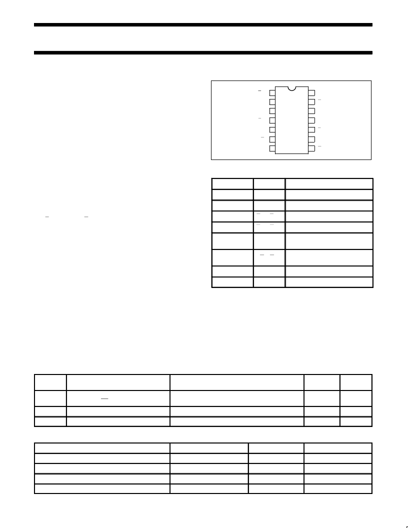
PIN CONFIGURATION
14
13
12
11
10
9
8
7
6
5
4
3
2
1
GND
V
CC
SD1
Q1
Q1
CP1
RD1
D1
RD0
D0
Q0
CP0
SD0
Q0
SA00001
PIN DESCRIPTION
PIN NUMBER
SYMBOL
NAME AND FUNCTION
2, 12
D0, D1
Data inputs
3, 11
CP0, CP1
Clock inputs (active rising edge)
4, 10
SD0, SD1
Set inputs (active-Low)
1, 13
RD0, RD1
Reset inputs (active-Low)
5, 9
Q0, Q1
Data outputs (active-Low),
non-inverting
6, 8
Q0, Q1
Data outputs (active-Low),
inverting
7
GND
Ground (0V)
14
V
CC
Positive supply voltage
QUICK REFERENCE DATA
SYMBOL
PARAMETER
CONDITIONS
T
amb
= 25
°
C; GND = 0V
TYPICAL
UNIT
t
PLH
t
PHL
Propagation delay
CPn to Qn or Qn
C
L
= 50pF; V
CC
= 5V
2.8
2.4
ns
C
IN
Input capacitance
V
I
= 0V or V
CC
3
pF
I
CC
Total supply current
Outputs disabled; V
CC
=5.5V
2
μ
A
ORDERING INFORMATION
PACKAGES
TEMPERATURE RANGE
ORDER CODE
DRAWING NUMBER
14-pin plastic DIP
–40
°
C to +85
°
C
74ABT5074N
SOT27-1
14-pin plastic SOL
–40
°
C to +85
°
C
74ABT5074D
SOT108-1
14-pin plastic shrink small outline SSOP Type II
–40
°
C to +85
°
C
74ABT5074DB
SOT337-1
14-pin plastic thin shrink small outline (TSSOP) Type I
–40
°
C to +85
°
C
74ABT5074PW
SOT402-1
相關(guān)PDF資料 |
PDF描述 |
|---|---|
| 74ABT5074N | Synchronizing dual D-type flip-flop with metastable immune characteristics |
| 74ABT5074PW | Synchronizing dual D-type flip-flop with metastable immune characteristics |
| 74ABT5074DB | Synchronizing dual D-type flip-flop with metastable immune characteristics |
| 74ABT534APWDH | Octal D-type flip-flop, inverting 3-State |
| 74ABT534A | Octal D-type flip-flop, inverting(3-State)(八反相(三態(tài))D觸發(fā)器) |
相關(guān)代理商/技術(shù)參數(shù) |
參數(shù)描述 |
|---|---|
| 74ABT5074DB | 制造商:PHILIPS 制造商全稱:NXP Semiconductors 功能描述:Synchronizing dual D-type flip-flop with metastable immune characteristics |
| 74ABT5074DB-T | 制造商:未知廠家 制造商全稱:未知廠家 功能描述:Dual D-Type Flip-Flop |
| 74ABT5074D-T | 制造商:未知廠家 制造商全稱:未知廠家 功能描述:Dual D-Type Flip-Flop |
| 74ABT5074N | 制造商:PHILIPS 制造商全稱:NXP Semiconductors 功能描述:Synchronizing dual D-type flip-flop with metastable immune characteristics |
| 74ABT5074PW | 制造商:PHILIPS 制造商全稱:NXP Semiconductors 功能描述:Synchronizing dual D-type flip-flop with metastable immune characteristics |
發(fā)布緊急采購,3分鐘左右您將得到回復(fù)。