- 您現(xiàn)在的位置:買賣IC網(wǎng) > PDF目錄24563 > 673GP-26.000MHZ-QQK (FOX ELECTRONICS) TCXO, CLIPPED SINE OUTPUT, 26 MHz PDF資料下載
參數(shù)資料
| 型號: | 673GP-26.000MHZ-QQK |
| 廠商: | FOX ELECTRONICS |
| 元件分類: | TCXO, sine |
| 英文描述: | TCXO, CLIPPED SINE OUTPUT, 26 MHz |
| 封裝: | ROHS COMPLIANT, SMD, 4 PIN |
| 文件頁數(shù): | 1/1頁 |
| 文件大?。?/td> | 150K |
| 代理商: | 673GP-26.000MHZ-QQK |
15
FOXElectronics 5570 Enterprise Parkway Fort Myers, Florida 33905 USA +1.239.693.0099 FAX +1.239.693.1554 http://www.foxonline.com
EMEA Tel/Fax: +44 .1767.312632 | Asia Hong Kong Tel: +852.2854.4285 Fax +852.2854.4282 | Japan Tel: +81.3.3374.2079 Fax: +81.3.3374.5221
2009 FOX ELECTRONICS | ISO9001:2000 Certified
1.8V~3.3V, Clipped SINE, SMD TCXO/VCTCXO
FEATURES
0.5PPM Stability
Supply Voltages of 1.8V ~ 3.3V
1.2 mm Max Height
Clipped SINE Output
Supply
Voltage (Vdd
)
TCXO/VCTCXO
TCXO
VCTCXO
TCXO
VCTCXO
TCXO
VCTCXO
TCXO
VCTCXO
TCXO
VCTCXO
TCXO
VCTCXO
Model
Number
FOX923C-GP
FOX923CE-GP
FOX923B-GP
FOX923E-GP
FOX923D-GP
FOX923DE-GP
FOX923F-GP
FOX923FE-GP
FOX923G-GP
FOX923GE-GP
FOX923L-GP
FOX923LE-GP
Part Number
673CGP-Frequency-xxxxx
638CGP-Frequency-xxxxx
673GP-Frequency-xxxxx
638GP-Frequency-xxxxx
673DGP-Frequency-xxxxx
638DGP-Frequency-xxxxx
673FGP-Frequency-xxxxx
638FGP-Frequency-xxxxx
673GGP-Frequency-xxxxx
638GGP-Frequency-xxxxx
673LGP-Frequency-xxxxx
638LGP-Frequency-xxxxx
3.3V ±5%
3.3V ±5%
3.0V ±5%
2.8V ±5%
2.7V ±5%
2.5V ±5%
1.8V ±5%
PART NUMBER SELECTION Learn More - Internet Required
1For proper operation, a control Voltage (Vc) must be applied to pin 1 on VCTCXO's.
2Does not imply a stocked part. All frequencies may not be available for all Vdd
.
3Other fequencies may be available. Contact Fox Technical support with your requirements.
*Dimensional drawing is for reference to critical specifications defined by size measurements.
Certain non-critical visual attributes, such as side castellations, reference pin shape, etc. may very.
All specifications subject to change without notice.
OPTIONS
Voltage Control
SMD TCXO/VCTCXO for GPS Applications
Rev. 6/30/2009
RoHS Compliant / Pb Free
Model: FOX923_-GP SERIES
Page 1 of 1
#1
#4
#3
#2
#1
#2
#4
#3
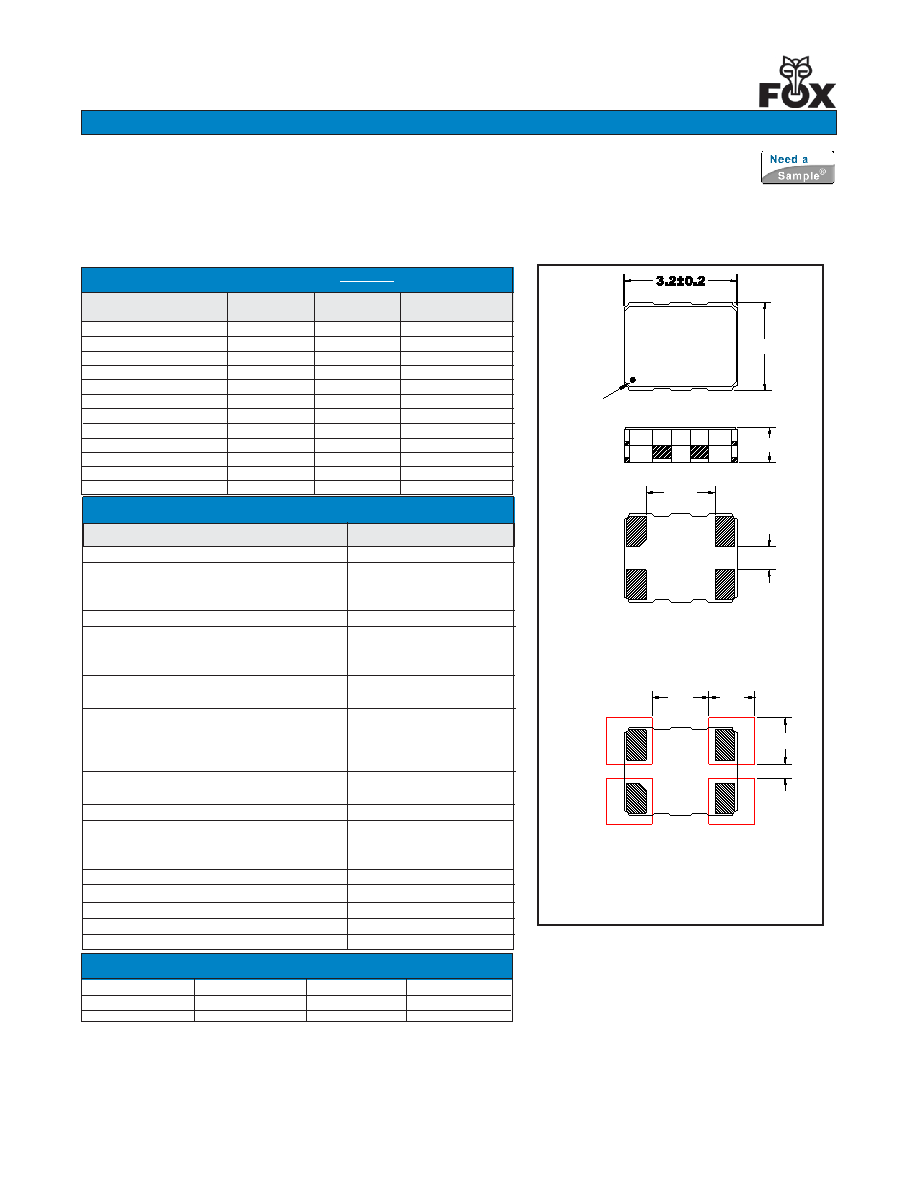
2.5±0.2
1.95
0.65
1.6
1.3
0.4
Recom m ended
Solder Pad Layout
Marking
Top
View
Bottom
View
Dot denotes
pin 1.
All dimensions are in millimeters.
Pin Connections
TCXO
VCTCXO
#1 NC
#3 Output
#1Vc
#3 Output
#2 GND #4 VDD
1.2 Max
#4
#1
#3
#2
See Table Below
-30C ~ +85C
-40C ~ +90C
1.8V ~ 3.3V
1.5mA
1.7mA
±1.5 PPM
±0.5 PPM
±0.3 PPM
±0.2 PPM
0.8V Min
10K
±10% // 10pF ±10%
±5 ~ ±15PPM
±3 ~ ±5PPM
±1.0PPM
-145 dBc/Hz Typical
260C / 10 Seconds
1
Au
PARAMETERS
Frequency Range
(Fo)
Temperature Range
Operating
(Topr)
Storage
(Tstg)
Supply Voltage
(Vdd)
Input Current
(Idd)
Fo = 16.3676 ~ 23.104MHz
Fo = 24.5535 ~ 27.456MHz
Initial Frequency Tolerance @ 25C (after 2 reflows)
(VCTCXO: Vc
= 0.5Vdd)1
Frequency Stability
Over Temperature Range
Over Supply Voltage Change (Vdd ± 5%)
Over Load Change (10K ±10%//10pF±10%)
Output Waveform
(Clipped Sine)
Peak-to-Peak Level (Vp-p)
Output Load
Pullability
Vdd = 2.5V~3.3V, Vc = 50% Vdd ±1.0V
Vdd = 1.8V, Vc = 0.9V ±0.6V
Aging per year
Phase Noise (26.000MHz, @ 10kHz offset)
Reflow Soldering Temp
Moisture Sensitivity Level (MSL)
Termination Finish
ELECTRICAL CHARACTERISTICS
MAX (unless otherwise noted)
STANDARD FREQUENCIES2&3
16.3676 MHz
16.369 MHz
24.5535 MHz
16.367677 MHz
19.200 MHz
27.456 MHz
16.367667 MHz
16.800 MHz
26.000 MHz
16.368 MHz
23.104 MHz
相關PDF資料 |
PDF描述 |
|---|---|
| 673LGP-16.800MHZ-QQK | TCXO, CLIPPED SINE OUTPUT, 16.8 MHz |
| 673LGP-19.200MHZ-QQK | TCXO, CLIPPED SINE OUTPUT, 19.2 MHz |
| 673GP-23.104MHZ-QQK | TCXO, CLIPPED SINE OUTPUT, 23.104 MHz |
| 673CGP-24.5535MHZ-QQK | TCXO, CLIPPED SINE OUTPUT, 24.5535 MHz |
| 673GGP-23.104MHZ-QQK | TCXO, CLIPPED SINE OUTPUT, 23.104 MHz |
相關代理商/技術參數(shù) |
參數(shù)描述 |
|---|---|
| 673H154-1 | 制造商:MINNESOTA MINING AND MFG 功能描述: 制造商:MN MIN 功能描述: |
| 673L-38.4-3 | 制造商:Fox Electronics 功能描述: 制造商:Fox Electronics 功能描述:FOX923L/38.4 - Cut Tape Product |
| 673L-38.4-8 | 制造商:Fox Electronics 功能描述:FOX923L/38.4 - Cut Tape Product |
| 673M-01ILF | 功能描述:鎖相環(huán) - PLL PLL BUILDING BLOCK RoHS:否 制造商:Silicon Labs 類型:PLL Clock Multiplier 電路數(shù)量:1 最大輸入頻率:710 MHz 最小輸入頻率:0.002 MHz 輸出頻率范圍:0.002 MHz to 808 MHz 電源電壓-最大:3.63 V 電源電壓-最小:1.71 V 最大工作溫度:+ 85 C 最小工作溫度:- 40 C 封裝 / 箱體:QFN-36 封裝:Tray |
| 673M-01ILFT | 功能描述:鎖相環(huán) - PLL PLL BUILDING BLOCK RoHS:否 制造商:Silicon Labs 類型:PLL Clock Multiplier 電路數(shù)量:1 最大輸入頻率:710 MHz 最小輸入頻率:0.002 MHz 輸出頻率范圍:0.002 MHz to 808 MHz 電源電壓-最大:3.63 V 電源電壓-最小:1.71 V 最大工作溫度:+ 85 C 最小工作溫度:- 40 C 封裝 / 箱體:QFN-36 封裝:Tray |
發(fā)布緊急采購,3分鐘左右您將得到回復。