- 您現(xiàn)在的位置:買賣IC網(wǎng) > PDF目錄360277 > 5962R9689104VXC (Aeroflex Inc.) Radiation-Hardened 32K x 8 PROM PDF資料下載
參數(shù)資料
| 型號: | 5962R9689104VXC |
| 廠商: | Aeroflex Inc. |
| 英文描述: | Radiation-Hardened 32K x 8 PROM |
| 中文描述: | 輻射加固32K的× 8胎膜早破 |
| 文件頁數(shù): | 2/11頁 |
| 文件大小: | 69K |
| 代理商: | 5962R9689104VXC |
2
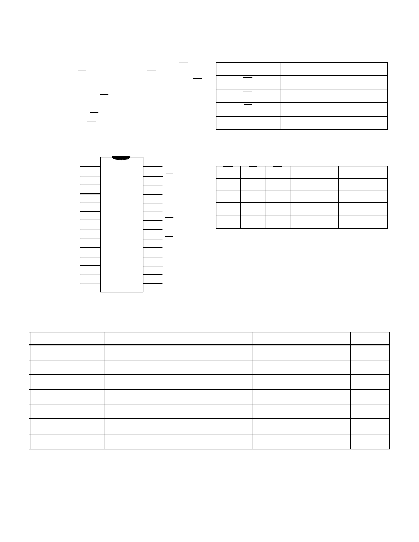
DEVICE OPERATION
The UT28F256 has three control inputs: Chip Enable (CE),
Program Enable (PE), and Output Enable (OE); fifteen address
inputs, A(14:0); and eight bidirectional data lines, DQ(7:0). CE
is the device enable input that controls chip selection, active, and
standby modes. Asserting CE causes I
DD
to rise to its active value
and decodes the fifteen address inputs to select one of 32,768
words in the memory. PE controls program and read operations.
During a read cycle, OE must be asserted to enable the outputs.
PIN NAMES
Table 1. Device Operation Truth Table
1
Notes:
1. “X” is defined as a “don’t care” condition.
2. Device active; outputs disabled.
ABSOLUTE MAXIMUM RATINGS
1
(Referenced to V
SS
)
Notes:
1. Stresses outside the listed absolute maximum ratings may cause permanent damage to the device. This is a stress rating only, and functional operation of the
device at these or any other conditions beyond limits indicated in the operational sections of this specification is not recommended. Exposure to
absolute maximum rating conditions for extended periods may affect device reliability.
2. Test per MIL-STD-883, Method 1012, infinite heat sink.
A14
A12
A7
A6
A5
A4
A3
A2
A1
A0
DQ0
DQ1
DQ2
V
SS
V
DD
PE
A13
A8
A9
A11
OE
A10
CE
DQ7
DQ6
DQ5
DQ4
DQ3
PIN CONFIGURATION
1
2
3
4
5
6
7
8
9
10
11
12
13
14
28
27
26
25
24
23
22
21
20
19
18
17
16
15
A(14:0)
Address
CE
Chip Enable
OE
Output Enable
PE
Program Enable
DQ(7:0)
Data Input/Data Output
OE
PE
CE
I/O MODE
MODE
X
1
1
Three-state
Standby
0
1
0
Data Out
Read
1
0
0
Data In
Program
1
1
0
Three-state
Read
2
SYMBOL
PARAMETER
LIMITS
UNITS
V
DD
DC supply voltage
-0.3 to 7.0
V
V
I/O
Voltage on any pin
-0.5 to (V
DD
+ 0.5)
V
T
STG
Storage temperature
-65 to +150
°
C
P
D
Maximum power dissipation
1.5
W
T
J
Maximum junction temperature
+175
°
C
Θ
JC
Thermal resistance, junction-to-case
2
3.3
°
C/W
I
I
DC input current
±
10
mA
相關PDF資料 |
PDF描述 |
|---|---|
| 5962F9689104VYX | Radiation-Hardened 32K x 8 PROM |
| 5962G9689104VYX | Radiation-Hardened 32K x 8 PROM |
| 5962H9689104VYX | Radiation-Hardened 32K x 8 PROM |
| 5962R9583403QXC | Quad Receiver |
| 5962R9583401VXA | ICSM, UPC2758TB-E3 SO6 2120 |
相關代理商/技術參數(shù) |
參數(shù)描述 |
|---|---|
| 5962R9863601VGA | 制造商:Analog Devices 功能描述: |
| 5962R9863602VGA | 制造商:Analog Devices 功能描述:OP AMP, JFET-INPUT - Rail/Tube |
| 5962R9863701VGA | 制造商:Analog Devices 功能描述:- Rail/Tube |
| 5962R9863701VHA | 制造商:Analog Devices 功能描述:AEROSPACE LOW INPUT CURRENT OPERATIONAL AMPLIFIER - Rail/Tube |
| 5962R9863701VPA | 制造商:Analog Devices 功能描述:OP AMP, GENERAL PURPOSE - Rail/Tube |
發(fā)布緊急采購,3分鐘左右您將得到回復。