- 您現(xiàn)在的位置:買賣IC網(wǎng) > PDF目錄156622 > 4565B2 ATM/SONET/SDH SUPPORT CIRCUIT, PBGA909 PDF資料下載
參數(shù)資料
| 型號: | 4565B2 |
| 元件分類: | 數(shù)字傳輸電路 |
| 英文描述: | ATM/SONET/SDH SUPPORT CIRCUIT, PBGA909 |
| 封裝: | PLASTIC, BGA-909 |
| 文件頁數(shù): | 29/61頁 |
| 文件大?。?/td> | 1691K |
| 代理商: | 4565B2 |
第1頁第2頁第3頁第4頁第5頁第6頁第7頁第8頁第9頁第10頁第11頁第12頁第13頁第14頁第15頁第16頁第17頁第18頁第19頁第20頁第21頁第22頁第23頁第24頁第25頁第26頁第27頁第28頁當(dāng)前第29頁第30頁第31頁第32頁第33頁第34頁第35頁第36頁第37頁第38頁第39頁第40頁第41頁第42頁第43頁第44頁第45頁第46頁第47頁第48頁第49頁第50頁第51頁第52頁第53頁第54頁第55頁第56頁第57頁第58頁第59頁第60頁第61頁
Hardware Design Guide, Revision 2
4565B Ultramapper Full Transport Retiming Device
December 17, 2003
622/155 Mbits/s SONET/SDH x DS3/E3/DS2/DS1/E1
Agere Systems Inc.
35
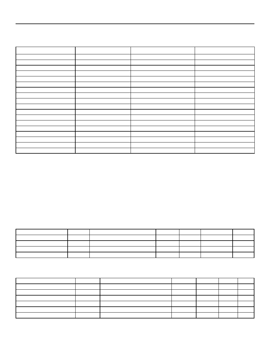
* Measured with a 50 MHz MPCLK. With a 25 MHz MPCLK, the typical per single instance value of MPU power is approximately 0.2 W.
Testing has shown that, on the average, approximately 0.35 W can be saved by utilizing the divide by 16 MPU clock power
down feature. Please refer to MPU register 0x0019 in the Ultramapper Register Description document for further information.
Additional MPU clock divisor options are available.
Additional power can be saved by powering down unused LVDS buffers. For details, please see MPU register 0x0026 in the
Ultramapper Register Description document.
4.4 ac and dc Characteristics
4.4.1 LVCMOS Interface Characteristics
Table 4-3. Typical Power Consumption Per Block
Typical power by block refers to all instances being used.
Block
Maximum Instance
Typical, Per Single Instance
Unit
TMUX
1
0.120
W
STSPP
1
0.020
W
STSXC
1
0.200
W
MRXC
1
0.050
W
SPEMPR
6
0.009
W
STS1LT
3
0.028
W
VTMPR
3
0.015
W
E13
3
0.013
W
M13
3
0.013
W
TPG/TPM
1
TBD
W
FRM
3
0.195
W
DS1DJA
3
0.026
W
DS3DJA
1
0.050
W
MPU
1
0.420*
W
CDR/PLL
1
0.150
W
LVDS I/O
15
0.020
W
NSMI I/O
3
0.032
W
DS3 I/O
6
0.050
W
Table 4-4. LVCMOS Inputs Specifications
Parameter
Symbol
Conditions
Min
Typ
Max
Unit
Input Leakage Current
II
VSS < VIN < VDD33
—
1.0*
A
High-input Voltage
VIH
—2.0
—
V
Low-input Voltage
VIL
—VSS
—0.8
V
Input Capacitance
CI
——
—
1.5
pF
* Excludes current due to pull-up or pull-down resistors.
Table 4-5. LVCMOS Outputs Specifications
Parameter
Symbol
Conditions
Min
Typ
Max
Unit
Output Voltage Low
VOL
IOL = max
VSS
—0.5
V
Output Voltage High
VOH
IOL = max
VDD – 0.5
—
VDD
V
Output Current Low
IOL
——
—
6*
mA
Output Current High
IOH
——
—
–6