- 您現(xiàn)在的位置:買賣IC網(wǎng) > PDF目錄33475 > 2SJ546-E 15 A, 60 V, 0.155 ohm, P-CHANNEL, Si, POWER, MOSFET, TO-220AB PDF資料下載
參數(shù)資料
| 型號: | 2SJ546-E |
| 元件分類: | JFETs |
| 英文描述: | 15 A, 60 V, 0.155 ohm, P-CHANNEL, Si, POWER, MOSFET, TO-220AB |
| 封裝: | TO-220CFM, 3 PIN |
| 文件頁數(shù): | 5/8頁 |
| 文件大?。?/td> | 88K |
| 代理商: | 2SJ546-E |

LA7358
No.A0638-5/17
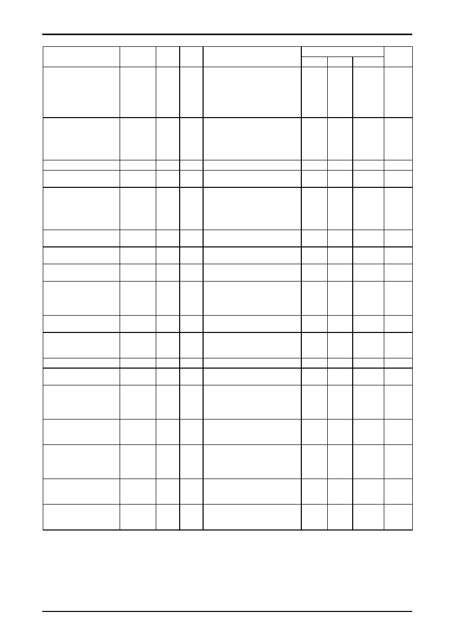
Continued from preceding page.
Ratings
Parameter
Symbol
Input
Test
point
Conditions
min
typ
max
Unit
PB chroma signal output
unwanted spectrum (1)
GSP1
S13
T17
SW1 = ON, V1 = 5V, V5 = V6 = 0V,
V16 = 5V, S13 = sine wave
(50mVp-p, f = 1.1MHz)
SW8B = ON, S27 = Comp.Sync
Measure 2.2MHz component at T17.
Referenced (0dB) to VOP.
-25
-15
dB
PB chroma signal output
unwanted spectrum (2)
GSP2
S13
T17
Same as above,
Note that S13 = sine wave
(50mVp-p, f = 1.1MHz)
Measure 3.3MHz component at T17.
Referenced (0dB) to VOP.
-20
-10
dB
CLK input level
VCLK
S2
f = 4.433619MHz
100
200
800
mVp-p
Sync signal input
threshold level
VTHS
S27
1.8
2
2.2
V
REC mode sync gate
start time (MUTE OFF)
TRGB
S27
T11
SW1 = ON, V1 = 5V, V5 = V6 = 0V,
V16 = 0V, S15 = sine wave
(200mVp-p, 4.286MHz)
SW21B = ON,
S27 = Comp.Sync (Note7)
-0.3
0.2
0.7
s
REC mode sync gate
start time (MUTE ON)
TRGBM
S27
T11
Same as above,
Note that SW2 = ON
1.5
2
2.5
s
REC mode sync gate
release time
TRGE
S27
T11
Same as above.
4.5
5.0
5.5
s
REC mode
mute setting resistance
VTSP2
S15
T17
(Note8)
10
20
30
k
PB mode sync gate
start time
TPGB
S27
T17
SW1 = ON, V5 = V6 =0V,
SW8B = ON, S13 = sine wave
(50mVp-p, f = 1.0715MHz)
V16 = 5V, S27 = Comp.Sync (Note9)
1.5
2
2.5
s
PB mode sync gate
release time
TPGE
S27
T17
Same as above.
4.5
5.0
5.5
s
BGP start time
TBGB
S27
T26
V5 = 0V, V6 = 5V, SW21B = ON,
V16 = 0V
S27 = Comp.Sync (Note10)
6.4
6.55
6.7
s
BGP width
TBGW
S27
T26
Same as above.
2.3
2.5
2.7
s
SECAM detection output
resistance
R26
T26
SW25 = ON, V25 = 5V (Note11)
7
10
13
k
REC mode
SECAM detection
characteristics (1)
VSCMR1
S15
T26
V5 = V6 =0V, V17 = 0V,
SW21B = ON, S27 = Comp.Sync
S15 = SECAM colour bar signal
(Note12)
4.5
V
REC mode
SECAM detection
characteristics (2)
VSCMR2
S15
T26
Same as above,
Note that S15 = PAL colour bar signal
(Note13)
0.5
V
PB mode phase detection
output differential voltage (1)
VSCPD1
S13
T23
T24
V5 = V6 = 0V, SW8B = ON, V16 = 5V,
S27 = Comp.Sync, S13 = sine wave
(50mVp-p, f = 1.0625/1.1016MHz)
(Note14)
150
180
mV
PB mode phase detection
output differential voltage (2)
VSCPD2
S14
T25
T26
Same as above,
Note tha S13 = sine wave
(50mVp-p, f = 627kHz) (Note14)
100
mV
PB mode phase detection
output differential voltage (3)
VSCPD3
S14
T25
T26
Same as above,
Note tha S13 = sine wave
(50mVp-p, f = 0.7/1.04MHz) (Note14)
100
mV
Continued on next page.
相關(guān)PDF資料 |
PDF描述 |
|---|---|
| 2SJ546-E | 15 A, 60 V, 0.155 ohm, P-CHANNEL, Si, POWER, MOSFET, TO-220AB |
| 2SJ546 | 0.155 ohm, POWER, FET |
| 2SJ548 | 15 A, 60 V, 0.155 ohm, P-CHANNEL, Si, POWER, MOSFET, TO-220AB |
| 2SJ551L-E | 18 A, 60 V, 0.11 ohm, P-CHANNEL, Si, POWER, MOSFET |
| 2SJ551STL-E | 18 A, 60 V, 0.11 ohm, P-CHANNEL, Si, POWER, MOSFET |
相關(guān)代理商/技術(shù)參數(shù) |
參數(shù)描述 |
|---|---|
| 2SJ547 | 制造商:HITACHI 制造商全稱:Hitachi Semiconductor 功能描述:Silicon P Channel MOS FET High Speed Power Switching |
| 2SJ547-E | 制造商:Renesas Electronics Corporation 功能描述: |
| 2SJ548 | 制造商:HITACHI 制造商全稱:Hitachi Semiconductor 功能描述:Silicon P Channel MOS FET High Speed Power Switching |
| 2SJ548-E | 制造商:Renesas Electronics Corporation 功能描述: |
| 2SJ549 | 制造商:HITACHI 制造商全稱:Hitachi Semiconductor 功能描述:Silicon P Channel MOS FET High Speed Power Switching |
發(fā)布緊急采購,3分鐘左右您將得到回復(fù)。