- 您現(xiàn)在的位置:買賣IC網(wǎng) > PDF目錄33474 > 2SJ492-ZJ 20 A, 60 V, 0.185 ohm, P-CHANNEL, Si, POWER, MOSFET, TO-263AB PDF資料下載
參數(shù)資料
| 型號: | 2SJ492-ZJ |
| 元件分類: | JFETs |
| 英文描述: | 20 A, 60 V, 0.185 ohm, P-CHANNEL, Si, POWER, MOSFET, TO-263AB |
| 封裝: | TO-263, 3 PIN |
| 文件頁數(shù): | 7/10頁 |
| 文件大?。?/td> | 266K |
| 代理商: | 2SJ492-ZJ |
LA4815VH
No.A1374-6/15
Notes on Using the IC
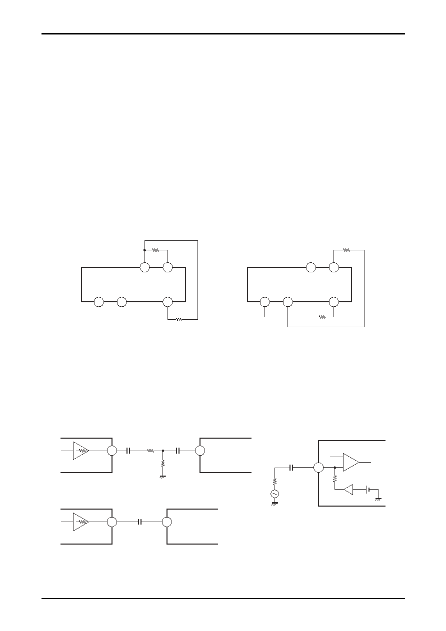
1. Voltage gain settings (Pins 4 and 11)
The voltage gain of the power amplifier is fixed by the internal resistors.
Pins 4 and 11 be left open : Approximately 26dB
Pins 4 and 11 connected to GND : Approximately 39.5dB
Note that the voltage gain can be changed using two resistors. (See Fig. 1)
Voltage gain setting : According to the resistor connected between Pin 4 and Pin 12 (GND1)
* Voltage gain = 20log (20
× (625 + Rvg1)/(125 + Rvg1))
Output DC voltage setting : According to the resistor connected between Pin 11 and Pin 12 (GND1)
* Rvg1 = Rvg2 must be satisfied.
In addition, the voltage gain can also be lowered to approximately 20dB (when using 5V or 6V power supply) by an
application such as shown in Fig. 2 below.
Voltage gain setting : According to the resistor connected between Pin 4 and Pin 1 (OUT)
* Voltage gain = 20log (20
× (125 + Rvg3)/(10,125 + Rvg3))
Output DC voltage setting : According to the resistor connected between Pin 11 and Pin 2 (VCC)
* Set the resistor values so that the Pin 5 (OUT) DC voltage is approximately half the supply voltage.
Example : When Rvg3 = 10k
, Rvg4 = 22k (when VCC = 6V)
However, note that using this method to greatly lower the voltage gain deteriorates the characteristics, so the voltage
gain should be lowered only to approximately 20dB. In addition, when using a high supply voltage (7V or more), the
clipped waveform may invert, so this voltage gain reduction method must not be used in these cases.
Figure 1
Figure 2
2. Signal source impedance : rg
As mentioned above, since the input coupling capacitor Cin affects the ripple rejection ratio, the signal source
impedance value rg, which is associated with this capacitor, also affects the ripple rejection ratio, so rg should be as
small as possible. Therefore, when attenuating the signal at the Cin front end as shown in Fig. 4, the constants should be
set in consideration of these characteristics. Using the smallest resistor Rg1 value possible is recommended.
In addition, when setting the signal level, the voltage gain should be set on the LA4815VH side and the input front-end
should be configured using only the input coupling capacitor, Cin, as shown in Fig. 5 in order to maximize the ripple
rejection ratio.
Figure 4
Figure 3
Figure 5
LA4815VH
Rvg2
Rvg1
GAIN2
OUT
VCC
GND1
GAIN1
LA4815VH
Rvg4
Rvg3
GAIN2
OUT
VCC
GND1
GAIN1
1
2
4
12
11
1
2
4
12
11
Vbias
100k
+
-
Pre-Amp
Rg2
Cin
Rg1
rg
other IC
ro
LA4815VH
Cin
other IC
ro
LA4815VH
Cin
IN
OUT
IN
13
OUT
IN
13
相關(guān)PDF資料 |
PDF描述 |
|---|---|
| 2SJ492-S | 20 A, 60 V, 0.185 ohm, P-CHANNEL, Si, POWER, MOSFET, TO-262AA |
| 2SJ496 | SMALL SIGNAL, FET |
| 2SJ496 | 5000 mA, 60 V, P-CHANNEL, Si, SMALL SIGNAL, MOSFET, TO-92 |
| 2SJ496 | 5000 mA, 60 V, P-CHANNEL, Si, SMALL SIGNAL, MOSFET, TO-92 |
| 2SJ505(L) | 0.036 ohm, POWER, FET |
相關(guān)代理商/技術(shù)參數(shù) |
參數(shù)描述 |
|---|---|
| 2SJ493 | 制造商:NEC 制造商全稱:NEC 功能描述:SWITCHING P-CHANNEL POWER MOS FET INDUSTRIAL USE |
| 2SJ494 | 制造商:NEC 制造商全稱:NEC 功能描述:SWITCHING P-CHANNEL POWER MOS FET INDUSTRIAL USE |
| 2SJ494-AZ | 制造商:Renesas Electronics 功能描述:Pch -60V -20A 50m@10V IsolatedTO220 Bulk 制造商:Renesas Electronics Corporation 功能描述:SEMICONDUCTOR, DESCRETE, MOS, FET, P CHA |
| 2SJ495 | 制造商:NEC 制造商全稱:NEC 功能描述:SWITCHING P-CHANNEL POWER MOS FET INDUSTRIAL USE |
| 2SJ495-AZ | 制造商:Renesas Electronics 功能描述:Cut Tape 制造商:Renesas Electronics 功能描述:Pch -60V -30A 30m@10V IsolatedTO220 Bulk 制造商:Renesas Electronics Corporation 功能描述:SEMICONDUCTOR, DESCRETE, MOS, FET, P CHA 制造商:Renesas 功能描述:Trans MOSFET P-CH 60V 30A 3-Pin(3+Tab) TO-220 Isolated |
發(fā)布緊急采購,3分鐘左右您將得到回復(fù)。