- 您現(xiàn)在的位置:買賣IC網 > PDF目錄33466 > 2SJ185 100 mA, 50 V, P-CHANNEL, Si, SMALL SIGNAL, MOSFET PDF資料下載
參數資料
| 型號: | 2SJ185 |
| 元件分類: | 小信號晶體管 |
| 英文描述: | 100 mA, 50 V, P-CHANNEL, Si, SMALL SIGNAL, MOSFET |
| 封裝: | MINIMOLD, SC-59, 3 PIN |
| 文件頁數: | 3/7頁 |
| 文件大小: | 353K |
| 代理商: | 2SJ185 |
The information in this document is subject to change without notice. Before using this document, please
confirm that this is the latest version.
Not all products and/or types are available in every country. Please check with an NEC Electronics
sales representative for availability and additional information.
1991
MOS FIELD EFFECT TRANSISTOR
2SJ185
P-CHANNEL MOSFET
FOR SWITCHING
DATA SHEET
Document No. D17903EJ3V0DS00 (3rd edition)
(Previous No. TC-2320)
Date Published February 2006 NS CP(K)
Printed in Japan
The mark <R> shows major revised points.
The revised points can be easily searched by copying an "<R>" in the PDF file and specifying it in the "Find what:" field.
The 2SJ185 is a P-channel vertical type MOSFET which can be
driven by 2.5 V power supply.
The 2SJ185 is driven by low voltage and does not require
consideration of driving current, it is suitable for appliances
including VTR cameras and headphone stereos which need
power saving.
FEATURES
Directly driven by ICs having a 3 V power supply.
Not necessary to consider driving current because of its high
input impedance.
Possible to reduce the number of parts by omitting the bias
resistor.
Complementary to 2SK1399
ORDERING INFORMATION
PART NUMBER
PACKAGE
2SJ185
SC-59 (Mini Mold)
Marking: H12
ABSOLUTE MAXIMUM RATINGS (TA = 25°C)
Drain to Source Voltage (VGS = 0 V)
VDSS
50
V
Gate to Source Voltage (VDS = 0 V)
VGSS
m7.0
V
Drain Current (DC)
ID(DC)
m100
mA
Drain Current (pulse)
Note
ID(pulse)
m200
mA
Total Power Dissipation
PT
200
mW
Storage Temperature
Tstg
55 to +150
°C
Note PW
≤ 10 ms, Duty Cycle ≤ 50%
Remark The diode connected between the gate and source of the transistor serves as a protector against ESD.
When this device actually used, an additional protection circuit is externally required if a voltage exceeding
the rated voltage may be applied to this device.
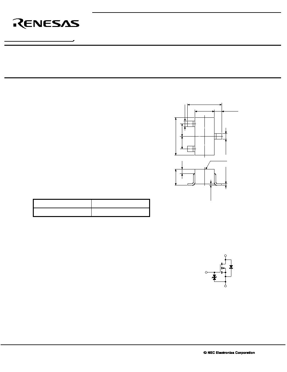
PACKAGE DRAWING (Unit: mm)
2.8 ±0.2
1.5
0.65
+0.1
–0.15
0.4
+0.1
–0.05
0.95
2.9
±0.2
0.4
+0.1
–0.05
0.3
1.1
to
1.4
Marking
0.16
+0.1
–0.06
0
to
0.1
1
2
3
1. Source
2. Gate
3. Drain
EQUIVALENT CIRCUIT
Source
Body
Diode
Gate
Protection
Diode
Gate
Drain
<R>
相關PDF資料 |
PDF描述 |
|---|---|
| 2SJ187(JA) | 1000 mA, 30 V, P-CHANNEL, Si, SMALL SIGNAL, MOSFET |
| 2SJ189TP | 4 A, 30 V, 0.17 ohm, P-CHANNEL, Si, POWER, MOSFET |
| 2SJ191TP | 2 A, 60 V, 0.6 ohm, P-CHANNEL, Si, POWER, MOSFET |
| 2SJ192 | 4 A, 60 V, 0.27 ohm, P-CHANNEL, Si, POWER, MOSFET |
| 2SJ195 | 4 A, 100 V, 0.55 ohm, P-CHANNEL, Si, POWER, MOSFET |
相關代理商/技術參數 |
參數描述 |
|---|---|
| 2SJ185-A | 制造商:Renesas Electronics Corporation 功能描述:SEMICONDUCTOR, DESCRETE, MOS, FET, P CHA |
| 2SJ185-T1B-A | 制造商:Renesas Electronics Corporation 功能描述:Trans MOSFET P-CH 50V 0.1A 3-Pin SC-59 T/R 制造商:Renesas Electronics Corporation 功能描述:SEMICONDUCTOR, DESCRETE, MOS, FET, P CHA |
| 2SJ186 | 制造商:HITACHI 制造商全稱:Hitachi Semiconductor 功能描述:Silicon P-Channel MOS FET |
| 2SJ186CY(TL-E) | 制造商:Renesas Electronics Corporation 功能描述: |
| 2SJ186CYEL-E | 制造商:RENESAS 制造商全稱:Renesas Technology Corp 功能描述:Silicon P Channel MOS FET |
發(fā)布緊急采購,3分鐘左右您將得到回復。