- 您現(xiàn)在的位置:買賣IC網(wǎng) > PDF目錄371435 > 28F1602C3 (Intel Corp.) 3 Volt Advanced+ Stacked Chip Scale Package Memory(3V閃速存儲器和靜態(tài)存儲器) PDF資料下載
參數(shù)資料
| 型號: | 28F1602C3 |
| 廠商: | Intel Corp. |
| 英文描述: | 3 Volt Advanced+ Stacked Chip Scale Package Memory(3V閃速存儲器和靜態(tài)存儲器) |
| 中文描述: | 3伏高級堆疊芯片級封裝存儲器(3V的閃速存儲器和靜態(tài)存儲器) |
| 文件頁數(shù): | 38/62頁 |
| 文件大小: | 538K |
| 代理商: | 28F1602C3 |
第1頁第2頁第3頁第4頁第5頁第6頁第7頁第8頁第9頁第10頁第11頁第12頁第13頁第14頁第15頁第16頁第17頁第18頁第19頁第20頁第21頁第22頁第23頁第24頁第25頁第26頁第27頁第28頁第29頁第30頁第31頁第32頁第33頁第34頁第35頁第36頁第37頁當前第38頁第39頁第40頁第41頁第42頁第43頁第44頁第45頁第46頁第47頁第48頁第49頁第50頁第51頁第52頁第53頁第54頁第55頁第56頁第57頁第58頁第59頁第60頁第61頁第62頁
28F1602C3, 28F3204C3
E
38
PRODUCT PREVIEW
V
CC
V
PP
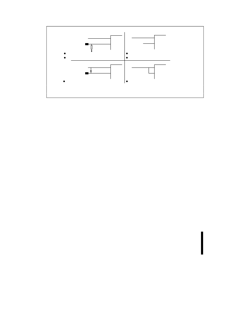
12 V Fast Programming
Absolute Write Protection With V
PP
≤
V
PPLK
System Supply
12 V Supply
10
≤
K
V
CC
V
PP
System Supply
12 V Supply
Low Voltage and 12 V Fast Programming
V
CC
V
PP
System Supply
Prot#
(Logic Signal)
V
CC
V
PP
System Supply
Low-Voltage Programming
Low-Voltage Programming
Absolute Write Protection via Logic Signal
(Note 1)
NOTE:
1.
A resistor can be used if the F-V
CC
supply can sink adequate current based on resistor value.
Figure 12. Example Power Supply Configurations
11.3
Noise Reduction
Stacked-CSP
characteristics require careful device decoupling.
System designers should consider three supply
current issues for both the flash and SRAM:
memory’s
power
switching
1.
2.
3.
Standby current levels (I
CCS
)
Read current levels (I
CCR
)
Transient peaks produced by falling and rising
edges of F-CE#, S-CS
1
#, and S-CS
2
.
Transient current magnitudes depend on the device
outputs’ capacitive and inductive loading. Two-line
control and proper decoupling capacitor selection
will suppress these transient voltage peaks. Each
device should have a 0.1 μF ceramic capacitor
connected between each F-V
CC
/S-V
CC
and GND,
and between its F-V
PP
and GND. These high-
frequency, inherently low-inductance capacitors
should be placed as close as possible to the
package leads.
Noise issues within a system can cause devices to
operate erratically if it is not adequately filtered. In
order to avoid any noise interaction issues within a
system, it is recommended that the design contain
the appropriate number of decoupling capacitors in
the system. Noise issues can also be reduced if
leads to the device are kept very short, in order to
reduce inductance.
Decoupling capacitors between V
and V
reduce
voltage spikes by supplying the extra current
needed during switching. Placing these capacitors
as close to the device as possible reduces line
inductance.
The
capacitors
inductance capacitors; surface mount capacitors
typically exhibit lower inductance.
should
be
low
相關(guān)PDF資料 |
PDF描述 |
|---|---|
| 28F3204C3 | 3 V Advanced+ Stacked Chip Scale Package Memory(3V高級堆芯片封裝存儲器) |
| 28F1604C3 | 3 Volt Advanced+ Stacked Chip Scale Package Memory(3V閃速存儲器和靜態(tài)存儲器) |
| 28F160C18 | 1.8V Advanced+ Boot Block Flash Memory(1.8V高級引導塊閃速存儲器) |
| 28F160C2 | 2.4V Advanced+ Boot Block Flash Memory(2.4V高級引導塊閃速存儲器) |
| 28F800C2 | 2.4V Advanced+ Boot Block Flash Memory(2.4V高級引導塊閃速存儲器) |
相關(guān)代理商/技術(shù)參數(shù) |
參數(shù)描述 |
|---|---|
| 28F160B3 | 制造商:INTEL 制造商全稱:Intel Corporation 功能描述:SMART 3 ADVANCED BOOT BLOCK 4-, 8-, 16-, 32-MBIT FLASH MEMORY FAMILY |
| 28F160BJHE-BTLTH | 制造商: 功能描述: 制造商:undefined 功能描述: |
| 28F160C3 | 制造商:INTEL 制造商全稱:Intel Corporation 功能描述:3 Volt Intel Advanced+ Boot Block Flash Memory |
| 28F160C3BA90 | 制造商: 功能描述: 制造商:Intel 功能描述: 制造商:undefined 功能描述: |
| 28F160C3TD70 | 制造商: 功能描述: 制造商:undefined 功能描述: |
發(fā)布緊急采購,3分鐘左右您將得到回復。