- 您現(xiàn)在的位置:買(mǎi)賣IC網(wǎng) > PDF目錄106295 > 110H1001-2RD6 1-OUTPUT AC-DC REG PWR SUPPLY MODULE PDF資料下載
參數(shù)資料
| 型號(hào): | 110H1001-2RD6 |
| 元件分類: | 電源模塊 |
| 英文描述: | 1-OUTPUT AC-DC REG PWR SUPPLY MODULE |
| 封裝: | 168.50 X 111.20 MM, 38.70 MM HEIGHT, METAL, CASE H02, MODULE |
| 文件頁(yè)數(shù): | 4/16頁(yè) |
| 文件大小: | 358K |
| 代理商: | 110H1001-2RD6 |
第1頁(yè)第2頁(yè)第3頁(yè)當(dāng)前第4頁(yè)第5頁(yè)第6頁(yè)第7頁(yè)第8頁(yè)第9頁(yè)第10頁(yè)第11頁(yè)第12頁(yè)第13頁(yè)第14頁(yè)第15頁(yè)第16頁(yè)

Benign Environment
AC-DC Converters <100 W
H-Family
Edition 2/96 - Melcher AG
10 - 73
MELCHER
The Power Partners.
10.3
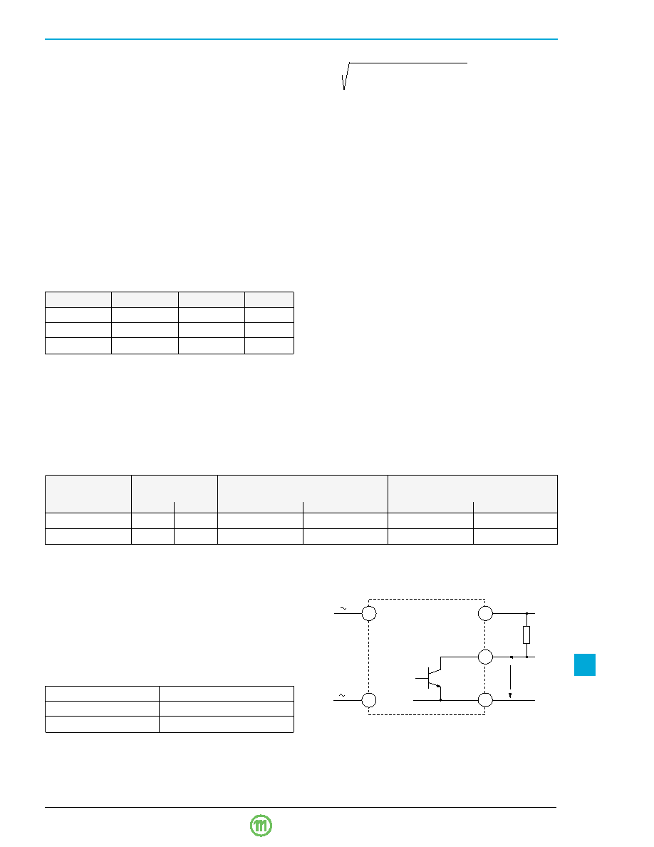
Formula for threshold level for desired value of
th:
2
Po (th + 0.3 ms) 100
Uti
=
––––––––––––––––––––– +
Ui min2
Ci min η
where as:
Ci min = minimum internal input capacitance [mF], accord-
ing to table below
Po
= output power [W]
h
= efficiency [%]
th
= hold-up time [ms]
Ui min = minimum input voltage [V]
Uti
= threshold level [V]
Remarks:
The threshold level
Uti of option V2 and V3 is adjusted dur-
ing manufacture to a value according to table "Undervol-
tage monitor functions", section "Option D").
A decoupling diode should be connected in series with the
input to avoid the input capacitance discharging through
other loads connected to the same source voltage.
Option V ACFAIL signal (VME)
This option defines an undervoltage monitoring circuit
for the input or the input and main output voltage
(
Uo1 nom = 5.1 V only) equivalent to option D and generates
the ACFAIL signal (V signal) which conforms to the VME
standard. The low state level of the ACFAIL signal is speci-
fied at a sink current of
IV = 48 mA to UV ≤ 0.6 V (open-col-
lector output of a NPN transistor). The pull-up resistor feed-
ing the open-collector output should be placed on the VME
backplane.
After the ACFAIL signal has gone low, the VME standard
requires a hold-up time
t h of at least 4 ms before the 5.1 V
output drops to 4.875 V when the 5.1 V output is fully
loaded. This hold-up time
th is provided by the internal input
capacitance. Consequently the working input voltage and
the threshold level
U ti should be adequately above the mini-
mum input voltage
Ui min of the converter so that enough
energy is remaining in the input capacitance.
Table 15: Undervoltage monitor functions
V output
Monitoring
Minimum adjustment range
Typical hysteresis
Uh [ % of Ut]
(VME compatible)
Ui
Uo1
of threshold level
Ut
for
Ut min...Ut max
Uti
Uto
Uhi
Uho
V2
yes
no
Ui min...Ui max 1–
3.0...0.5
-
V3
yes
Ui min...Ui max 1
0.95...0.98
Uo1 2
3.0...0.5
"0"
1 Threshold level adjustable by potentiometer (not recommended for mobile applications)
2 Fixed value between 95% and 98% of Uo1 (tracking), output undervoltage monitoring is not a requirement of VME standard
V output (V2, V3):
Connector pin V is internally connected to the open collec-
tor of a NPN transistor. The emitter is connected to the
negative potential of output 1.
UV ≤ 0.6 V (logic low) corre-
sponds to a monitored voltage level (
Ui and/or Uo1) < Ut.
The current
I V through the open collector should not exceed
50 mA. The NPN output is not protected against external
overvoltages.
UV should not exceed 80 V.
Ui, Uo1 status
V output,
UV
Ui or Uo1 < Ut
low, L,
UV ≤ 0.6 V at IV = 50 mA
Ui and Uo1 > Ut + Uh
high, H,
I V
≤ 25 A at UV = 5.1 V
20
23
5
Vo1+
Vo1–
V
UV
IV
N
29
32
Rp
P
Fig. 14
Output configuration of options V2 and V3
voltage(s) exceed(s)
Ut + Uh. The threshold level Ut is ad-
justable by a potentiometer accessible through a hole in the
front cover.
Versions V2 and V3 are available as shown below.
Option V operates independently of the built-in input under-
voltage lock-out circuit. A logic "low" signal is generated at
pin 5 as soon as one of the monitored voltages drops below
the preselected threshold level
Ut. The return for this signal
is Vo1– (pin 23). The V output recovers when the monitored
Table 14: Factory potentiometer setting of Uti
Types
110H
230H
Unit
Ci min
0.25
0.05
mF
Uti
94
200
V DC
t h
55
ms
相關(guān)PDF資料 |
PDF描述 |
|---|---|
| 153-10552G | 1-OUTPUT DC-DC REG PWR SUPPLY MODULE |
| 153-10555J | 2-OUTPUT DC-DC REG PWR SUPPLY MODULE |
| 153-10559H | 2-OUTPUT DC-DC REG PWR SUPPLY MODULE |
| 12AV200D | 2-OUTPUT 0.625 W DC-DC UNREG PWR SUPPLY MODULE |
| 110H2320-2D8 | 2-OUTPUT AC-DC REG PWR SUPPLY MODULE |
相關(guān)代理商/技術(shù)參數(shù) |
參數(shù)描述 |
|---|---|
| 110-HB | 制造商:STAEDTLER 功能描述:PENCIL HB BX12 制造商:STAEDTLER 功能描述:PENCIL, HB, BX12 |
| 110HBKT | 制造商:Vishay Spectrol 功能描述:BRACKET HORIZONTAL |
| 110HBKT | 制造商:Vishay Spectrol 功能描述:BRACKET HORIZONTAL |
| 110HBKT | 制造商:Vishay Spectrol 功能描述:BRACKET HORIZONTAL |
| 110-I | 功能描述:罩類、盒類及殼類產(chǎn)品 RoHS:否 制造商:Bud Industries 產(chǎn)品:Boxes 外部深度:6.35 mm 外部寬度:6.35 mm 外部高度:2.56 mm NEMA 額定值: IP 等級(jí): 材料:Acrylonitrile Butadiene Styrene (ABS) 顏色:Red |
發(fā)布緊急采購(gòu),3分鐘左右您將得到回復(fù)。