- 您現在的位置:買賣IC網 > PDF目錄382789 > μPD78075BY (NEC Corp.) 8 Bit Single Chip Microcontrollers PDF資料下載
參數資料
| 型號: | μPD78075BY |
| 廠商: | NEC Corp. |
| 元件分類: | 8位微控制器 |
| 英文描述: | 8 Bit Single Chip Microcontrollers |
| 中文描述: | 8位單片機微控制器 |
| 文件頁數: | 134/415頁 |
| 文件大小: | 1374K |
| 代理商: | ΜPD78075BY |
第1頁第2頁第3頁第4頁第5頁第6頁第7頁第8頁第9頁第10頁第11頁第12頁第13頁第14頁第15頁第16頁第17頁第18頁第19頁第20頁第21頁第22頁第23頁第24頁第25頁第26頁第27頁第28頁第29頁第30頁第31頁第32頁第33頁第34頁第35頁第36頁第37頁第38頁第39頁第40頁第41頁第42頁第43頁第44頁第45頁第46頁第47頁第48頁第49頁第50頁第51頁第52頁第53頁第54頁第55頁第56頁第57頁第58頁第59頁第60頁第61頁第62頁第63頁第64頁第65頁第66頁第67頁第68頁第69頁第70頁第71頁第72頁第73頁第74頁第75頁第76頁第77頁第78頁第79頁第80頁第81頁第82頁第83頁第84頁第85頁第86頁第87頁第88頁第89頁第90頁第91頁第92頁第93頁第94頁第95頁第96頁第97頁第98頁第99頁第100頁第101頁第102頁第103頁第104頁第105頁第106頁第107頁第108頁第109頁第110頁第111頁第112頁第113頁第114頁第115頁第116頁第117頁第118頁第119頁第120頁第121頁第122頁第123頁第124頁第125頁第126頁第127頁第128頁第129頁第130頁第131頁第132頁第133頁當前第134頁第135頁第136頁第137頁第138頁第139頁第140頁第141頁第142頁第143頁第144頁第145頁第146頁第147頁第148頁第149頁第150頁第151頁第152頁第153頁第154頁第155頁第156頁第157頁第158頁第159頁第160頁第161頁第162頁第163頁第164頁第165頁第166頁第167頁第168頁第169頁第170頁第171頁第172頁第173頁第174頁第175頁第176頁第177頁第178頁第179頁第180頁第181頁第182頁第183頁第184頁第185頁第186頁第187頁第188頁第189頁第190頁第191頁第192頁第193頁第194頁第195頁第196頁第197頁第198頁第199頁第200頁第201頁第202頁第203頁第204頁第205頁第206頁第207頁第208頁第209頁第210頁第211頁第212頁第213頁第214頁第215頁第216頁第217頁第218頁第219頁第220頁第221頁第222頁第223頁第224頁第225頁第226頁第227頁第228頁第229頁第230頁第231頁第232頁第233頁第234頁第235頁第236頁第237頁第238頁第239頁第240頁第241頁第242頁第243頁第244頁第245頁第246頁第247頁第248頁第249頁第250頁第251頁第252頁第253頁第254頁第255頁第256頁第257頁第258頁第259頁第260頁第261頁第262頁第263頁第264頁第265頁第266頁第267頁第268頁第269頁第270頁第271頁第272頁第273頁第274頁第275頁第276頁第277頁第278頁第279頁第280頁第281頁第282頁第283頁第284頁第285頁第286頁第287頁第288頁第289頁第290頁第291頁第292頁第293頁第294頁第295頁第296頁第297頁第298頁第299頁第300頁第301頁第302頁第303頁第304頁第305頁第306頁第307頁第308頁第309頁第310頁第311頁第312頁第313頁第314頁第315頁第316頁第317頁第318頁第319頁第320頁第321頁第322頁第323頁第324頁第325頁第326頁第327頁第328頁第329頁第330頁第331頁第332頁第333頁第334頁第335頁第336頁第337頁第338頁第339頁第340頁第341頁第342頁第343頁第344頁第345頁第346頁第347頁第348頁第349頁第350頁第351頁第352頁第353頁第354頁第355頁第356頁第357頁第358頁第359頁第360頁第361頁第362頁第363頁第364頁第365頁第366頁第367頁第368頁第369頁第370頁第371頁第372頁第373頁第374頁第375頁第376頁第377頁第378頁第379頁第380頁第381頁第382頁第383頁第384頁第385頁第386頁第387頁第388頁第389頁第390頁第391頁第392頁第393頁第394頁第395頁第396頁第397頁第398頁第399頁第400頁第401頁第402頁第403頁第404頁第405頁第406頁第407頁第408頁第409頁第410頁第411頁第412頁第413頁第414頁第415頁
108
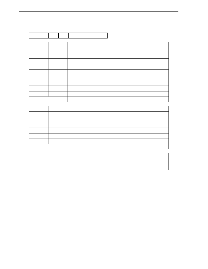
CHAPTER 5 APPLICATIONS OF 16-BIT TIMER/EVENT COUNTER
Figure 5-2. Format of Timer Clock Select Register 0 (
μ
PD78098, 78098B subseries)
TCL03 TCL02 TCL01 TCL00
Selects clock of PCL output
0
0
0
0
f
XT
(32.768 kHz)
0
1
0
1
f
XX
(4.0 MHz)
0
1
1
0
f
XX
/2 (2.0 MHz)
0
1
1
1
f
XX
/2
2
(1.0 MHz)
1
0
0
0
f
XX
/2
3
(500 kHz)
1
0
0
1
f
XX
/2
4
(250 kHz)
1
0
1
0
f
XX
/2
5
(125 kHz)
1
0
1
1
f
XX
/2
6
(62.5 kHz)
1
1
0
0
f
XX
/2
7
(31.3 kHz)
Others
Setting prohibited
TCL06 TCL05 TCL04
Selects count clock of 16-bit timer register
0
0
0
TI00 (valid edge can be specified)
0
0
1
2f
XX
Note
0
1
0
f
XX
(4.0 MHz)
0
1
1
f
XX
/2 (2.0 MHz)
1
0
0
f
XX
/2
2
(1.0 MHz)
1
1
1
Watch timer output (INTTM3)
Others
Setting prohibited
CLOE
Controls PCL output
0
Disables output
1
Enables output
Note
At f
XX
> 2.5 MHz, setting prohibited.
Cautions 1. The valid edge of the TI00/INTP0 pin is specified by the external interrupt mode register 0
(INTM0). The frequency of the sampling clock is selected by the sampling clock select register
(SCS).
2. To enable PCL output, set TCL00 through TCL03, and then set CLOE to 1 by using a 1-bit
memory manipulation instruction.
3. Read the count value from TM0, not from the capture/compare register 01(CR01), when TI00
is specified as the count clock of TM0.
4. Before writing new data to TCL0, stop the timer operation once.
Remarks 1.
f
XX
: main system clock frequency
: subsystem clock oscillation frequency
3.
TI00: input pin of 16-bit timer/event counter
4.
TM0 : 16-bit timer register
5.
( ) : at f
XX
= 4.0 MHz or f
XT
= 32.768 kHz
2.
f
XT
7
6
5
4
3
2
Symbol
1
0
FF40H
TCL00
TCL0
TCL01
TCL03 TCL02
TCL04
TCL05
TCL06
CLOE
Address
At reset
R/W
00H
R/W
相關PDF資料 |
PDF描述 |
|---|---|
| μPD78098 | 8 Bit Single Chip Microcontrollers |
| μPD78098B | 8 Bit Single Chip Microcontrollers |
| μPD780948GF | 8 Bit Microcontrollers(8 位微控制器) |
| μPD780949GF | 8 Bit Microcontrollers(8 位微控制器) |
| μPD78F0948GF | 8 Bit Microcontrollers(8 位微控制器) |
相關代理商/技術參數 |
參數描述 |
|---|---|
| PD784054GCA2 | 制造商:NEC 制造商全稱:NEC 功能描述:16-BIT SINGLE-CHIP MICROCONTROLLER |
| PD784976A | 制造商:NEC 制造商全稱:NEC 功能描述:16-Bit Single-Chip Microcontroller |
| PD7869 | 制造商:未知廠家 制造商全稱:未知廠家 功能描述:Optoelectronic |
| PD78F0134 | 制造商:NEC 制造商全稱:NEC 功能描述:8-Bit Single-Chip Microcontrollers |
| PD78F0134(A) | 制造商:NEC 制造商全稱:NEC 功能描述:8-Bit Single-Chip Microcontrollers |
發(fā)布緊急采購,3分鐘左右您將得到回復。