- 您現(xiàn)在的位置:買賣IC網(wǎng) > PDF目錄382787 > μPD78074BY (NEC Corp.) 8 Bit Single Chip Microcontrollers(8位單片微控制器) PDF資料下載
參數(shù)資料
| 型號: | μPD78074BY |
| 廠商: | NEC Corp. |
| 英文描述: | 8 Bit Single Chip Microcontrollers(8位單片微控制器) |
| 中文描述: | 8位單片機微控制器(8位單片微控制器) |
| 文件頁數(shù): | 70/194頁 |
| 文件大小: | 863K |
| 代理商: | ΜPD78074BY |
第1頁第2頁第3頁第4頁第5頁第6頁第7頁第8頁第9頁第10頁第11頁第12頁第13頁第14頁第15頁第16頁第17頁第18頁第19頁第20頁第21頁第22頁第23頁第24頁第25頁第26頁第27頁第28頁第29頁第30頁第31頁第32頁第33頁第34頁第35頁第36頁第37頁第38頁第39頁第40頁第41頁第42頁第43頁第44頁第45頁第46頁第47頁第48頁第49頁第50頁第51頁第52頁第53頁第54頁第55頁第56頁第57頁第58頁第59頁第60頁第61頁第62頁第63頁第64頁第65頁第66頁第67頁第68頁第69頁當前第70頁第71頁第72頁第73頁第74頁第75頁第76頁第77頁第78頁第79頁第80頁第81頁第82頁第83頁第84頁第85頁第86頁第87頁第88頁第89頁第90頁第91頁第92頁第93頁第94頁第95頁第96頁第97頁第98頁第99頁第100頁第101頁第102頁第103頁第104頁第105頁第106頁第107頁第108頁第109頁第110頁第111頁第112頁第113頁第114頁第115頁第116頁第117頁第118頁第119頁第120頁第121頁第122頁第123頁第124頁第125頁第126頁第127頁第128頁第129頁第130頁第131頁第132頁第133頁第134頁第135頁第136頁第137頁第138頁第139頁第140頁第141頁第142頁第143頁第144頁第145頁第146頁第147頁第148頁第149頁第150頁第151頁第152頁第153頁第154頁第155頁第156頁第157頁第158頁第159頁第160頁第161頁第162頁第163頁第164頁第165頁第166頁第167頁第168頁第169頁第170頁第171頁第172頁第173頁第174頁第175頁第176頁第177頁第178頁第179頁第180頁第181頁第182頁第183頁第184頁第185頁第186頁第187頁第188頁第189頁第190頁第191頁第192頁第193頁第194頁
51
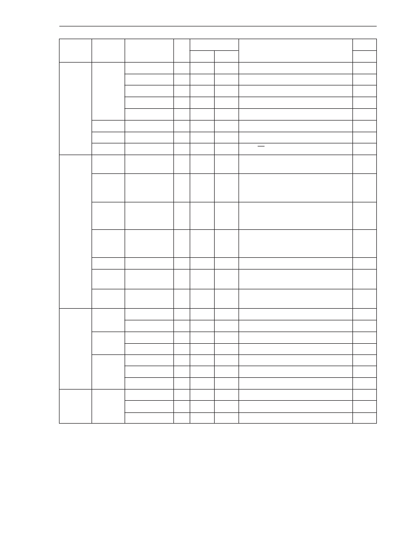
CHAPTER 4 INSTRUCTION SET
Bit
CLR1
saddr.bit
2
8
12
(saddr.bit)
←
0
Manipulation
sfr.bit
3
–
16
sfr.bit
←
0
A.bit
2
8
–
A.bit
←
0
PSW.bit
2
–
12
PSW.bit
←
0
×
×
×
[HL].bit
2
12
16+2n+2m
(HL).bit
←
0
SET1
CY
1
4
–
CY
←
1
1
CLR1
CY
1
4
–
CY
←
0
0
NOT1
CY
1
4
–
CY
←
CY
×
Call Return
CALL
!addr16
3
14
–
(SP–1)
←
(PC+3)
H
, (SP–2)
←
(PC+3)
L
,
PC
←
addr16, SP
←
SP–2
CALLF
!addr11
2
10
–
(SP–1)
←
(PC+2)
H
, (SP–2)
←
(PC+2)
L
,
PC
15–11
←
00001, PC
10–0
←
addr11,
SP
←
SP–2
CALLT
[addr5]
1
12
–
(SP–1)
←
(PC+1)
H
, (SP–2)
←
(PC+1)
L
,
PC
H
←
(00000000, addr5+1),
PC
L
←
(00000000, addr5), SP
←
SP–2
BRK
1
12
–
(SP–1)
←
PSW, (SP–2)
←
(PC+1)
H
,
(SP–3)
←
(PC+1)
L
, PC
H
←
(003FH),
PC
L
←
(003EH), SP
←
SP–3, IE
←
0
RET
1
12
–
PC
H
←
(SP+1), PC
L
←
(SP), SP
←
SP+2
RETI
1
12
–
PC
H
←
(SP+1), PC
L
←
(SP),
PSW
←
(SP+2), SP
←
SP+3, NMIS
←
0
R R R
RETB
1
12
–
PC
H
←
(SP+1), PC
L
←
(SP),
PSW
←
(SP+2), SP
←
SP+3
R R R
Stack
PUSH
PSW
1
4
–
(SP–1)
←
PSW, SP
←
SP–1
Manipulation
rp
1
8
–
(SP–1)
←
rp
H
, (SP–2)
←
rp
L
, SP
←
SP–2
POP
PSW
1
4
–
PSW
←
(SP), SP
←
SP+1
R R R
rp
1
8
–
rp
H
←
(SP+1), rp
L
←
(SP), SP
←
SP+2
MOVW
SP,#word
4
–
20
SP
←
word
SP, AX
2
–
16
SP
←
AX, SP
2
–
16
AX
←
SP
Unconditional
BR
!addr16
3
12
–
PC
←
addr16
Branch
$addr16
2
12
–
PC
←
PC+2+jdisp8
AX
2
16
–
PC
H
←
A, PC
L
←
X
Notes 1.
When the internal high-speed RAM area is accessed or in the instruction with no data access.
When an area except the internal high-speed RAM area is accessed.
2.
Remarks 1.
1 instruction clock cycle is 1 CPU clock cycle (f
CPU
) selected by the processor clock control register
(PCC).
Number of clock cycles is when there is a program in the internal ROM area.
n indicates the number of waits when the external memory expansion area is read.
m indicates the number of waits when the external memory expansion area is written to.
2.
3.
4.
Instruction
Group
Clock
Flag
Mnemonic
Operands
Byte
Operation
Note 1
Note 2
Z AC CY
相關PDF資料 |
PDF描述 |
|---|---|
| μPD78094 | 8 Bit Single Chip Microcontrollers(8位單片微控制器) |
| μPD78095 | 8 Bit Single Chip Microcontrollers(8位單片微控制器) |
| μPD78095B | 8 Bit Single Chip Microcontrollers(8位單片微控制器) |
| μPD78043F | 8 Bit Single Chip Microcontrollers(8位單片微控制器) |
| μPD78046F | 8Bit Single Chip Microcontrollers(8位單片微控制器) |
相關代理商/技術參數(shù) |
參數(shù)描述 |
|---|---|
| PD784054GCA2 | 制造商:NEC 制造商全稱:NEC 功能描述:16-BIT SINGLE-CHIP MICROCONTROLLER |
| PD784976A | 制造商:NEC 制造商全稱:NEC 功能描述:16-Bit Single-Chip Microcontroller |
| PD7869 | 制造商:未知廠家 制造商全稱:未知廠家 功能描述:Optoelectronic |
| PD78F0134 | 制造商:NEC 制造商全稱:NEC 功能描述:8-Bit Single-Chip Microcontrollers |
| PD78F0134(A) | 制造商:NEC 制造商全稱:NEC 功能描述:8-Bit Single-Chip Microcontrollers |
發(fā)布緊急采購,3分鐘左右您將得到回復。