- 您現(xiàn)在的位置:買賣IC網(wǎng) > PDF目錄382788 > μPD78056F (NEC Corp.) 8 Bit Single Chip Microcontrollers PDF資料下載
參數(shù)資料
| 型號: | μPD78056F |
| 廠商: | NEC Corp. |
| 元件分類: | 8位微控制器 |
| 英文描述: | 8 Bit Single Chip Microcontrollers |
| 中文描述: | 8位單片機(jī)微控制器 |
| 文件頁數(shù): | 60/76頁 |
| 文件大小: | 571K |
| 代理商: | ΜPD78056F |
第1頁第2頁第3頁第4頁第5頁第6頁第7頁第8頁第9頁第10頁第11頁第12頁第13頁第14頁第15頁第16頁第17頁第18頁第19頁第20頁第21頁第22頁第23頁第24頁第25頁第26頁第27頁第28頁第29頁第30頁第31頁第32頁第33頁第34頁第35頁第36頁第37頁第38頁第39頁第40頁第41頁第42頁第43頁第44頁第45頁第46頁第47頁第48頁第49頁第50頁第51頁第52頁第53頁第54頁第55頁第56頁第57頁第58頁第59頁當(dāng)前第60頁第61頁第62頁第63頁第64頁第65頁第66頁第67頁第68頁第69頁第70頁第71頁第72頁第73頁第74頁第75頁第76頁
60
μ
PD78056F, 78058F
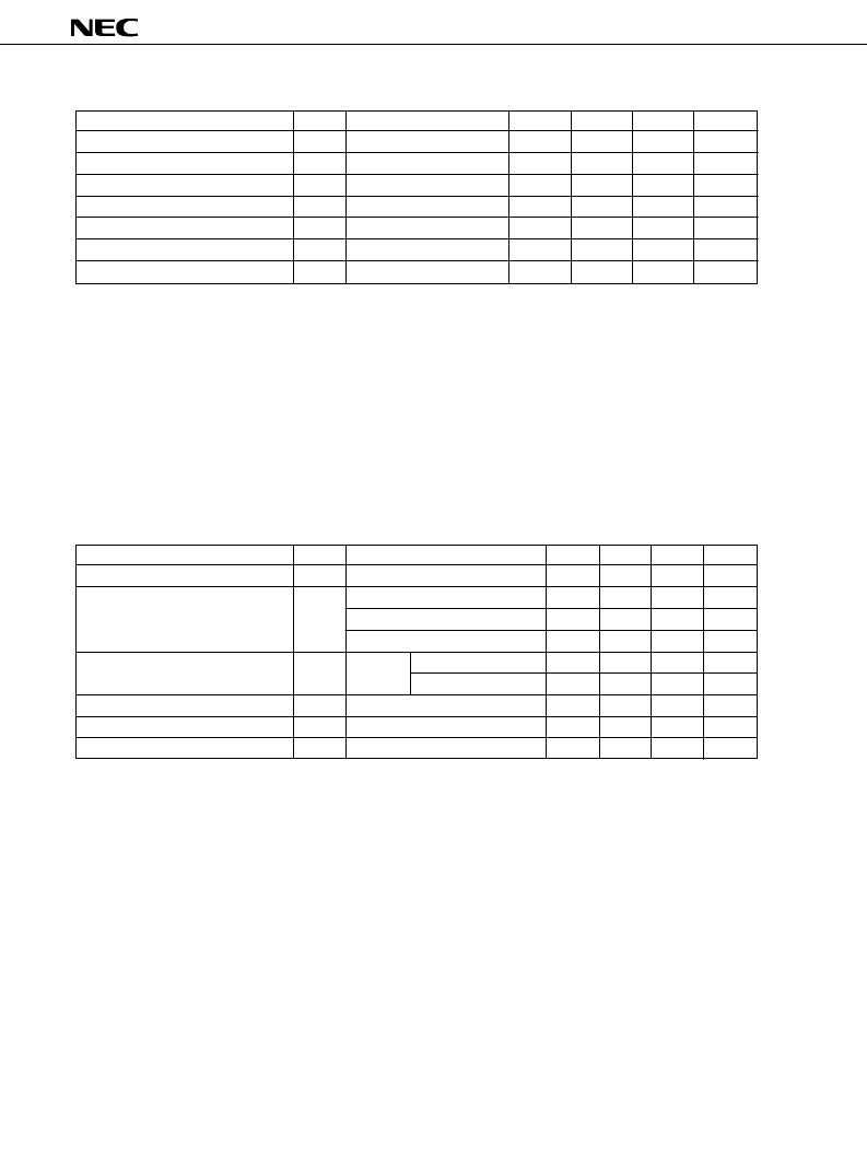
A/D CONVERTER CHARACTERISTICS (T
A
= –40 to +85
°
C, AV
DD
= V
DD
= 2.7 to 6.0 V, AV
SS
= V
SS
= 0 V)
Parameter
Symbol
Test Conditions
MIN.
TYP.
MAX.
Unit
8
8
8
bit
2.7 V
≤
AV
REF0
≤
AV
DD
0.6
%
t
CONV
19.1
200
μ
s
t
SAMP
12/f
xx
μ
s
V
IAN
AV
SS
AV
REF0
V
AV
REF0
2.7
AV
DD
V
R
AIREF0
4
14
k
Resolution
Overall error
Note
Conversion time
Sampling time
Analog input voltage
Reference voltage
Resistance between AV
REF0
and AV
SS
Resolution
Overall error
Settling time
Output resistance
Analog reference voltage
Resistance between AV
REF1
and AV
SS
Note
Overroll error excluding quantization error (
±
1/2 LSB). It is indicated as a ratio to the full-scale value.
Caution
For pins which also function as port pins (see 3.1 Port Pins), do not perform the following
operations during A/D conversion. If these operations are performed, the total error ratings
cannot be kept (except for LCD segment output alternate-function pin).
(1)
Rewrite the output latch while the pin is used as a port pin.
(2)
Change the output level of the pin used as an output pin, even if it is not used as a port pin.
Remarks
1.
2.
f
XX
: Main system clock frequency (f
X
or f
X
/2)
f
x
: Main system clock oscillation frequency
D/A CONVERTER CHARACTERISTICS (T
A
= –40 to +85
°
C, V
DD
= 2.7 to 6.0 V, AV
SS
= V
SS
= 0 V)
Parameter
Symbol
Test Conditions
MIN.
TYP.
MAX.
Unit
8
bit
R = 2M
Note 1
1.2
%
R = 4M
Note 1
R = 10M
Note 1
0.8
%
0.6
%
Note 1
4.5 V
≤
AV
REF1
≤
6.0 V
C=30pF
2.7 V
≤
AV
REF1
< 4.5 V
10
μ
s
15
μ
s
R
O
Note 2
10
k
AV
REF1
2.0
V
DD
V
R
AIREF1
DACS0, DACS1 = 55H
Note 2
4
8
k
Notes
1.
R and C are the load resistance and load capacitance of the D/A converter output pins.
2.
Value for D/A converter 1 channel
Remark
DACS0, DACS1: D/A conversion value setting register 0, 1
相關(guān)PDF資料 |
PDF描述 |
|---|---|
| μPD78058F | 8 Bit Single Chip Microcontrollers |
| μPD78056Y | 8Bit Single Chip Microcontrollers(8位單片微控制器) |
| μPD78052Y | 8Bit Single Chip Microcontrollers(8位單片微控制器) |
| μPD78053Y | 8Bit Single Chip Microcontrollers(8位單片微控制器) |
| μPD78054Y | 8Bit Single Chip Microcontrollers(8位單片微控制器) |
相關(guān)代理商/技術(shù)參數(shù) |
參數(shù)描述 |
|---|---|
| PD7-80-70A | 制造商:MERRIMAC 制造商全稱:MERRIMAC 功能描述:0 , 75 ohm POWER DIVIDERS / COMBINERS |
| PD784054GCA2 | 制造商:NEC 制造商全稱:NEC 功能描述:16-BIT SINGLE-CHIP MICROCONTROLLER |
| PD784976A | 制造商:NEC 制造商全稱:NEC 功能描述:16-Bit Single-Chip Microcontroller |
| PD7869 | 制造商:未知廠家 制造商全稱:未知廠家 功能描述:Optoelectronic |
| PD78F0134 | 制造商:NEC 制造商全稱:NEC 功能描述:8-Bit Single-Chip Microcontrollers |
發(fā)布緊急采購,3分鐘左右您將得到回復(fù)。