- 您現(xiàn)在的位置:買賣IC網(wǎng) > PDF目錄375052 > XQ4085XL-1BG475N (Xilinx, Inc.) QML High-Reliability FPGAs PDF資料下載
參數(shù)資料
| 型號: | XQ4085XL-1BG475N |
| 廠商: | Xilinx, Inc. |
| 英文描述: | QML High-Reliability FPGAs |
| 中文描述: | QML第高可靠性的FPGA |
| 文件頁數(shù): | 12/22頁 |
| 文件大?。?/td> | 162K |
| 代理商: | XQ4085XL-1BG475N |
QPRO XQ4000XL Series QML High-Reliability FPGAs
12
www.xilinx.com
1-800-255-7778
DS029 (v1.3) June 25, 2000
Product Specification
R
Output Flip-Flop, Clock to Out, BUFGEs 3, 4, 7, and 8
Capacitive Load Factor
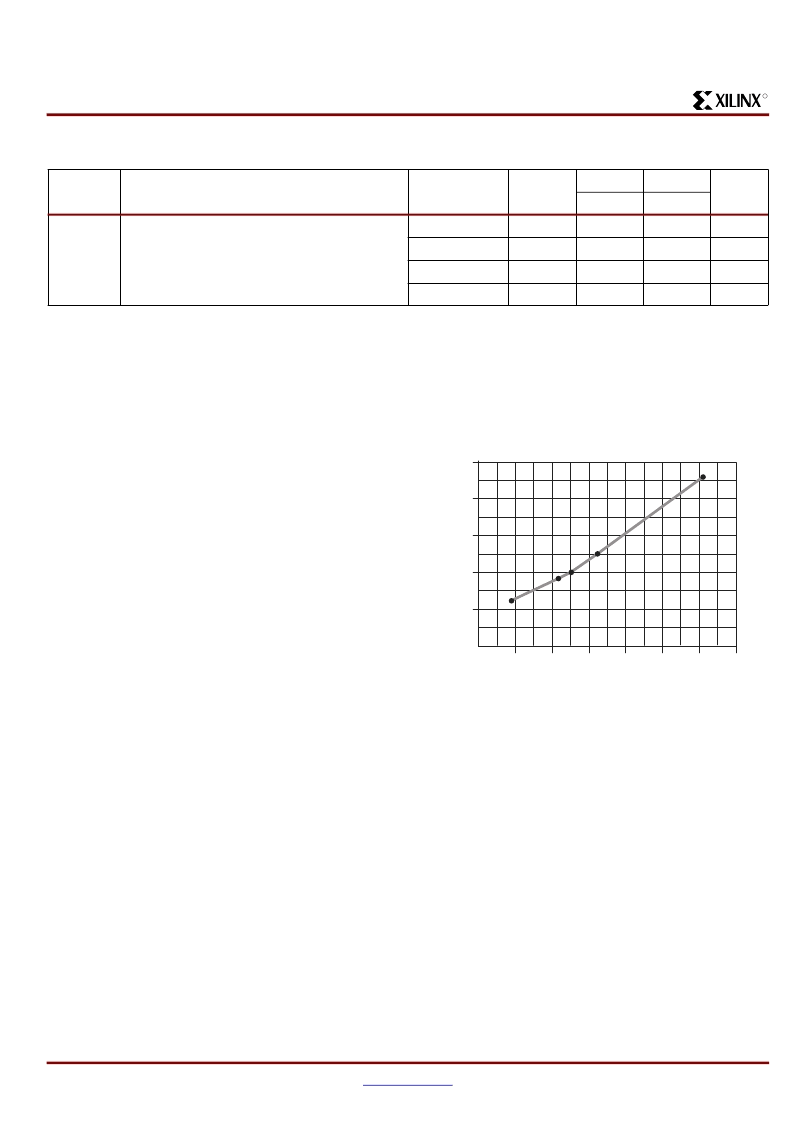
Figure 1
shows the relationship between I/O output delay
and load capacitance. It allows a user to adjust the specified
output delay if the load capacitance is different than 50 pF.
For example, if the actual load capacitance is 120 pF, add
2.5 ns to the specified delay. If the load capacitance is
20 pF, subtract 0.8 ns from the specified output delay.
Figure 1
is usable over the specified operating conditions of
voltage and temperature and is independent of the output
slew rate control.
Symbol
Description
Device
All
Min
-3
-1
Units
Max
Max
T
ICKEOF
Global early clock to output using OFF
Values are for BUFGEs 3, 4, 7, and 8.
XQ4013XL
1.8
8.8
-
ns
XQ4036XL
1.8
9.7
-
ns
XQ4062XL
2.0
10.9
-
ns
XQ4085XL
2.2
-
9.3
ns
Notes:
1.
Clock-to-out minimum delay is measured with the fastest route and the lightest load, Clock-to-out maximum delay is measured using
the farthest distance and a reference load of one clock pin (IK or OK) per IOB as well as driving all accessible CLB flip-flops. For
designs with a smaller number of clock loads, the pad-to-IOB clock pin delay as determined by the static timing analyzer (TRCE) can
be added to the AC parameter Tokpof and used as a worst-case pin-to-pin clock-to-out delay for clocked outputs for FAST mode
configurations.
Output timing is measured at ~50% V
CC
threshold with 50 pF external capacitive load.
2.
Figure 1:
Delay Factor at Various Capacitive Loads
DS029_03_011300
-2
0
20
40
60
80
Capacitance (pF)
D
100
120
140
-1
0
1
2
3
相關(guān)PDF資料 |
PDF描述 |
|---|---|
| XQ4085XL-1CB240M | QML High-Reliability FPGAs |
| XQ4085XL-1CB240N | QML High-Reliability FPGAs |
| XQ4085XL-1CB432M | QML High-Reliability FPGAs |
| XQ4085XL-1CB432N | QML High-Reliability FPGAs |
| XQ4085XL-1CB475M | QML High-Reliability FPGAs |
相關(guān)代理商/技術(shù)參數(shù) |
參數(shù)描述 |
|---|---|
| XQ4085XL-1CB228M | 制造商:XILINX 制造商全稱:XILINX 功能描述:QML High-Reliability FPGAs |
| XQ4085XL-1CB228N | 制造商:未知廠家 制造商全稱:未知廠家 功能描述:FPGA |
| XQ4085XL-1CB240M | 制造商:XILINX 制造商全稱:XILINX 功能描述:QML High-Reliability FPGAs |
| XQ4085XL-1CB240N | 制造商:XILINX 制造商全稱:XILINX 功能描述:QML High-Reliability FPGAs |
| XQ4085XL-1CB432M | 制造商:XILINX 制造商全稱:XILINX 功能描述:QML High-Reliability FPGAs |
發(fā)布緊急采購,3分鐘左右您將得到回復(fù)。