- 您現(xiàn)在的位置:買賣IC網(wǎng) > PDF目錄375044 > XQ2V1000 (Xilinx, Inc.) QPro Virtex-II 1.5V Military QML Platform FPGAs PDF資料下載
參數(shù)資料
| 型號: | XQ2V1000 |
| 廠商: | Xilinx, Inc. |
| 英文描述: | QPro Virtex-II 1.5V Military QML Platform FPGAs |
| 中文描述: | QPro的Virtex - II 1.5V的軍事QML第平臺FPGA |
| 文件頁數(shù): | 8/128頁 |
| 文件大小: | 2738K |
| 代理商: | XQ2V1000 |
第1頁第2頁第3頁第4頁第5頁第6頁第7頁當前第8頁第9頁第10頁第11頁第12頁第13頁第14頁第15頁第16頁第17頁第18頁第19頁第20頁第21頁第22頁第23頁第24頁第25頁第26頁第27頁第28頁第29頁第30頁第31頁第32頁第33頁第34頁第35頁第36頁第37頁第38頁第39頁第40頁第41頁第42頁第43頁第44頁第45頁第46頁第47頁第48頁第49頁第50頁第51頁第52頁第53頁第54頁第55頁第56頁第57頁第58頁第59頁第60頁第61頁第62頁第63頁第64頁第65頁第66頁第67頁第68頁第69頁第70頁第71頁第72頁第73頁第74頁第75頁第76頁第77頁第78頁第79頁第80頁第81頁第82頁第83頁第84頁第85頁第86頁第87頁第88頁第89頁第90頁第91頁第92頁第93頁第94頁第95頁第96頁第97頁第98頁第99頁第100頁第101頁第102頁第103頁第104頁第105頁第106頁第107頁第108頁第109頁第110頁第111頁第112頁第113頁第114頁第115頁第116頁第117頁第118頁第119頁第120頁第121頁第122頁第123頁第124頁第125頁第126頁第127頁第128頁
QPro Virtex-II 1.5V Military QML Platform FPGAs
8
www.xilinx.com
1-800-255-7778
DS122 (v1.1) January 7, 2004
Product Specification
R
All of the user IOBs have fixed-clamp diodes to V
CCO
and to
ground. As outputs, these IOBs are not compatible or com-
pliant with 5V I/O standards. As inputs, these IOBs are not
normally 5V tolerant, but can be used with 5V I/O standards
when external current-limiting resistors are used. For more
details, see the “5V Tolerant I/Os” Tech Topic at
http://www.xilinx.com
.
Table 8
lists supported I/O standards with Digitally Con-
trolled Impedance. See
Digitally Controlled Impedance
(DCI)
, page 13
.
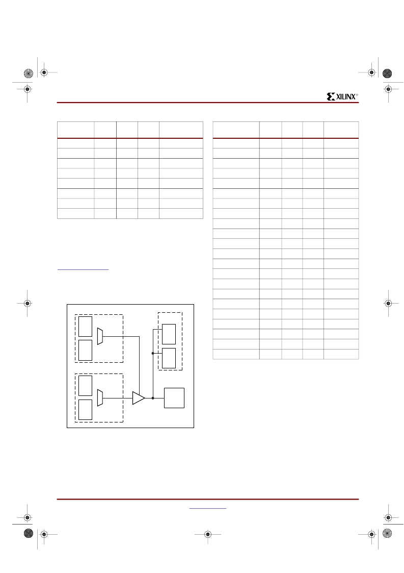
Logic Resources
IOB blocks include six storage elements, as shown in
Figure 3
.
Each storage element can be configured either as an
edge-triggered D-type flip-flop or as a level-sensitive latch.
On the input, output, and 3-state path, one or two DDR reg-
isters can be used.
Double data rate is directly accomplished by the two regis-
ters on each path, clocked by the rising edges (or falling
edges) from two different clock nets. The two clock signals
are generated by the DCM and must be 180 degrees out of
phase, as shown in
Figure 4
. There are two input, output,
and 3-state data signals, each being alternately clocked out.
Table 7:
Supported Differential Signal I/O Standards
I/O Standard
Output
V
CCO
Input
V
CCO
Input
V
REF
Output
V
OD
LVPECL_33
3.3
N/A
N/A
490 mV to 1.22V
LDT_25
2.5
N/A
N/A
0.430 - 0.670
LVDS_33
3.3
N/A
N/A
0.250 - 0.400
LVDS_25
2.5
N/A
N/A
0.250 - 0.400
LVDSEXT_33
3.3
N/A
N/A
0.330 - 0.700
LVDSEXT_25
2.5
N/A
N/A
0.330 - 0.700
BLVDS_25
2.5
N/A
N/A
0.250 - 0.450
ULVDS_25
2.5
N/A
N/A
0.430 - 0.670
Figure 3:
Virtex-II
IOB Block
Reg
OCK1
Reg
OCK2
Reg
ICK1
Reg
ICK2
DDR mux
Input
PAD
3-State
Reg
OCK1
Reg
OCK2
DDR mux
Output
IOB
DS031_29_100900
Table 8:
Supported DCI I/O Standards
I/O
Standard
Output
V
CCO
Input
V
CCO
Input
V
REF
Termination
Type
LVDCI_33
(1)
3.3
3.3
N/A
Series
LVDCI_DV2_33
(1)
3.3
3.3
N/A
Series
LVDCI_25
(1)
2.5
2.5
N/A
Series
LVDCI_DV2_25
(1)
2.5
2.5
N/A
Series
LVDCI_18
(1)
1.8
1.8
N/A
Series
LVDCI_DV2_18
(1)
1.8
1.8
N/A
Series
LVDCI_15
(1)
1.5
1.5
N/A
Series
LVDCI_DV2_15
(1)
1.5
1.5
N/A
Series
GTL_DCI
1.2
1.2
0.8
Single
GTLP_DCI
1.5
1.5
1.0
Single
HSTL_I_DCI
1.5
1.5
0.75
Split
HSTL_II_DCI
1.5
1.5
0.75
Split
HSTL_III_DCI
1.5
1.5
0.9
Single
HSTL_IV_DCI
1.5
1.5
0.9
Single
HSTL_I_DCI
1.8
N/A
0.9
Split
HSTL_II_DCI
1.8
N/A
0.9
Split
HSTL_III_DCI
1.8
N/A
1.1
Single
HSTL_IV_DCI
1.8
N/A
1.1
Single
SSTL2_I_DCI
(2)
2.5
2.5
1.25
Split
SSTL2_II_DCI
(2)
2.5
2.5
1.25
Split
SSTL3_I_DCI
(2)
3.3
3.3
1.5
Split
SSTL3_II_DCI
(2)
3.3
3.3
1.5
Split
Notes:
1.
LVDCI_XX and LVDCI_DV2_XX are LVCMOS controlled
impedance buffers, matching the reference resistors or half
of the reference resistors.
These are SSTL compatible.
2.
ds122_1_1.fm Page 8 Wednesday, January 7, 2004 9:15 PM
相關PDF資料 |
PDF描述 |
|---|---|
| XQ2V1000-4BG575M | QPro Virtex-II 1.5V Military QML Platform FPGAs |
| XQ2V1000-4BG575N | QPro Virtex-II 1.5V Military QML Platform FPGAs |
| XQ2V1000-4BG728M | QPro Virtex-II 1.5V Military QML Platform FPGAs |
| XQ2V1000-4BG728N | QPro Virtex-II 1.5V Military QML Platform FPGAs |
| XQ2V1000-4CF1144M | QPro Virtex-II 1.5V Military QML Platform FPGAs |
相關代理商/技術參數(shù) |
參數(shù)描述 |
|---|---|
| XQ2V1000_1 | 制造商:XILINX 制造商全稱:XILINX 功能描述:QPro Virtex-II 1.5V Platform FPGAs |
| XQ2V1000-4BG575M | 制造商:XILINX 制造商全稱:XILINX 功能描述:QPro Virtex-II 1.5V Military QML Platform FPGAs |
| XQ2V1000-4BG575N | 制造商:XILINX 制造商全稱:XILINX 功能描述:QPro Virtex-II 1.5V Military QML Platform FPGAs |
| XQ2V1000-4BG728M | 制造商:XILINX 制造商全稱:XILINX 功能描述:QPro Virtex-II 1.5V Military QML Platform FPGAs |
| XQ2V1000-4BG728N | 制造商:XILINX 制造商全稱:XILINX 功能描述:QPro Virtex-II 1.5V Military QML Platform FPGAs |
發(fā)布緊急采購,3分鐘左右您將得到回復。